Vacuum Grip End Effectors
Precision Wafer Handling Solutions for Semiconductor Manufacturing
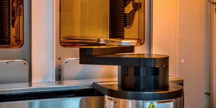
Overview
- Vacuum grip end effectors enable secure, non-contact wafer handling in advanced semiconductor environments.
- Designed for minimum particle generation
- Ensures stable wafer pickup through controlled vacuum flow
- Ideal for ultra‑clean, high‑precision wafer transfer
Key Features
-
Low‑particle, contamination‑controlled design
-
High repeatability for 200mm–300mm wafers
-
Optimized vacuum channels for uniform grip
-
Lightweight construction for smooth robot motion
Applications
-
Wafer loading/unloading
-
Metrology and inspection tools
-
Process tool transfers
-
Cleanroom automation systems
Benefits for Semiconductor Fabs
-
Reduced wafer damage risk
-
Higher tool uptime and throughput
-
Improved handling stability
-
Supports advanced automation and precision motion workflows
Why Choose Kensington Labs?
-
Proven reliability in wafer-handling systems
-
Precision engineering expertise
-
Custom end effector designs for unique fab needs
-
Over 40 years supporting semiconductor automation
Contact us
- Kensington Laboratories
-
Phone: +1 (925) 548-0640
-
Website: kensingtonlabs.com