Project
Design a Folded-cascode OpAmp
The Schematic

Get id from gain, bandwidth, and slew rate
f_u \approx f_{3dB} \times Av
= \frac{1}{2\pi R_{out}C_{out}} \times g_{m1,2}R_{out} \\
= \frac{g_{m1,2}}{2\pi C_{out}} \\
= \frac{I_{d1,2}}{\pi C_{out}V_{ov1,2}}
- Bandwidth & Gain
I_{d1,2} > f_u \pi C_{out} V_{ov1,2}
For target bandwidth,
- Slew Rate
I_2 = i_{d5-10}
\frac{I_{ss}}{2} = i_{d1,2}
I_1 = \frac{I_{ss}}{2} + I_2
SR_- = (I_2 - max\{(I_1 - I_{ss}), 0\}) / C_{out}
SR_+ = (I_1 - I_2) / C_{out}
- Let I1 - Iss <= 0, so I2 can be minimize.
- Also SR- = I2 / Cout
- Slew Rate (Continue)
I_1 \le I_{ss} \\
\rArr I_2 + \frac{I_{ss}}{2} \le I_{ss} \\
\rArr \frac{I_{ss}}{2} \ge I_2 = SR_- * C_{out}
\rArr I_{d1,2} \ge I_{d5-10} = SR_- * C_{out}
Let's recall previous result,
I_{d1,2} > f_u \pi C_{out} V_{ov1,2}
I_{d1,2} \ge I_{d5-10} = SR_- * C_{out}
Then, the minimal requirement will be,
I_{d1,2} = max\{ f_u \pi C_{out} V_{ov1,2}, SR_- * C_{out} \}
I_{d5-10} = SR_- * C_{out}
More about gain
Av = g_{m1}R_{out}
Now, gm1 is known, gain is given, Rout can be calculated.
R_{out} = r_{op} \parallel r_{on}
r_{op} = g_{m7}r_{o7}r_{o9}
r_{on} = g_{m5}(r_{o1} \parallel r_{o3})r_{o5}
Let
More about gain (Continue)
r_{op} = k * r_{on}
R_{out} = k*r_{on} \parallel r_{on} = \frac{k*r_{on}^2}{(k+1)r_{on}} \\
\rArr r_{on} = \frac{k+1}{k}R_{out} \\
\rArr r_{op} = (k+1)R_{out}
Get\ r_{op}\ and\ r_{on}\ from\ R_{out}
More about gain (Continue)
Get\ r_{o7-10}\ from\ r_{op} = g_{m7}r_{o7}r_{o9}
Let
r_{o7} = r_{o9}
\rArr r_{o7} = r_{o9} = \sqrt{\frac{r_{op}}{g_{m7}}}
More about gain (Continue)
Get\ r_{o1,3,5}\ from\ r_{on} = g_{m5}(r_{o1} \parallel r_{o3})r_{o5}
Let\ r_{o5} = m*(r_{o1} \parallel r_{o3}) \\
r_{o1} = n*(r_{o3})
Skip the calculation...
r_{o1} \parallel r_{o3} = \sqrt{\frac{r_{on}}{m*g_{m5}}} \\
r_{o5} = m*(r_{o1} \parallel r_{o3})
Text
More about gain (Continue)
All ro can be modeled as functions of Rout
when k, m, n are set
In my case, k = 6, m = 1.9, n = 4.
From ro to gate length
r_o = \frac{1+\lambda V_{ds}}{\lambda I_d}
Vds can be set and Id is known, we can calculate lambda.
The\ relationship\ of\ \lambda\ vs\ gate\ length\ can\ be\ get\ from\ simulation.
From gate length to width
I_d = 0.5 * \mu n,p * C_{ox} * \frac{W}{L} * V_{ov}^2 * (1 + \lambda V_{ds})
\mu_n * C_{ox} = 258 \mu A/V^2 \\
\mu_p * C_{ox} = 94 \mu A/V^2
From model parameters,
The Initial Design
I write an auto-generation tool, so complicated hand calculation can be avoided.
The tool is open-source:

The Final Design after fine-tuning
Mb1,b2: w=165u, l=0.22u
M1,2: w=360u, l=0.5u
M3,4: w=130u, l=0.9u
M5,6: w=85u, l=0.8u
M7,8: w=300u, l=0.56u
M9,10: w=55u, l=0.56u
Id1,2 = 700uA
Id5-10 = 515uA
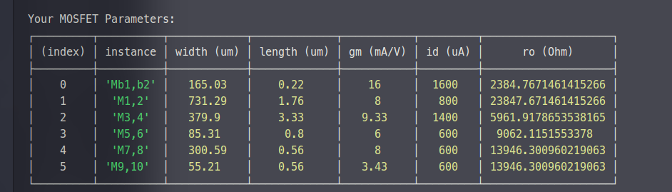
Simulation Results
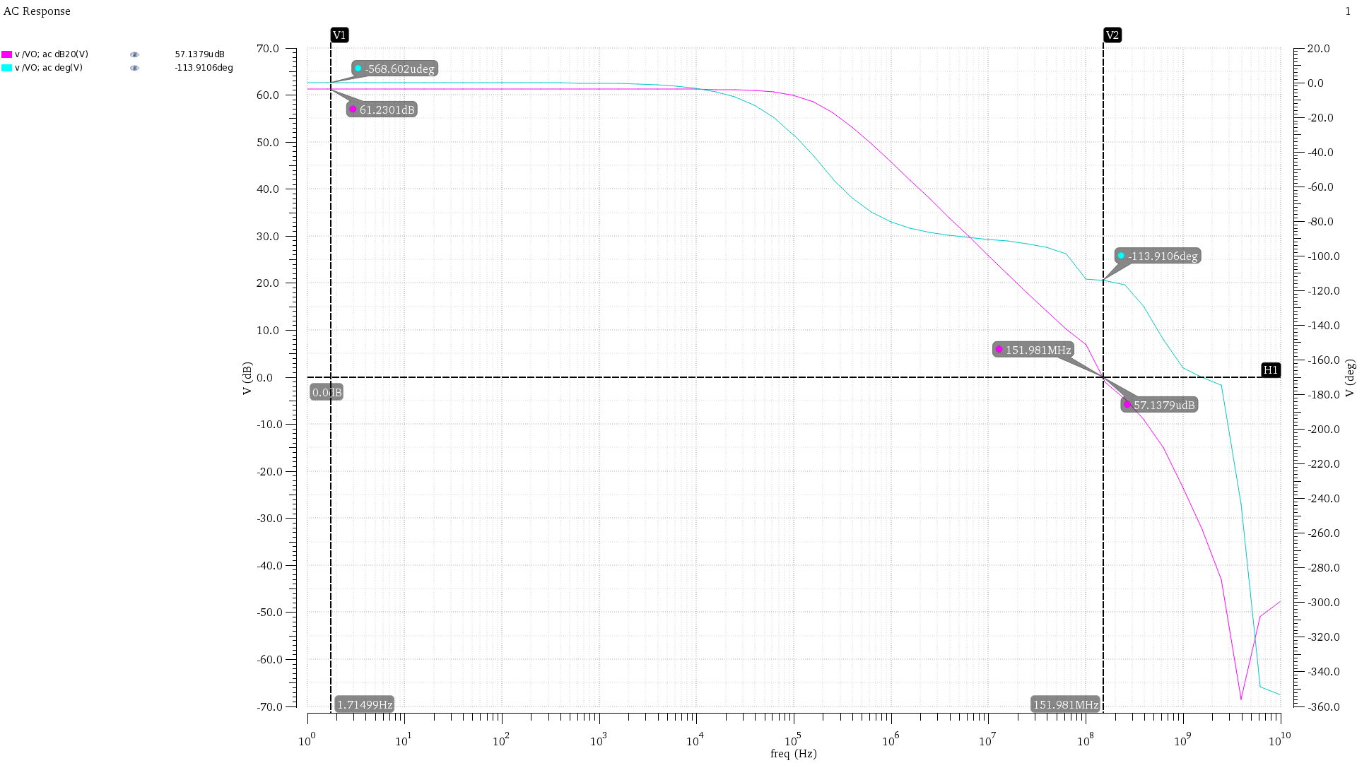
UGBW: 156MHz
PM: 67.3 degree
Gain: 61.6dB
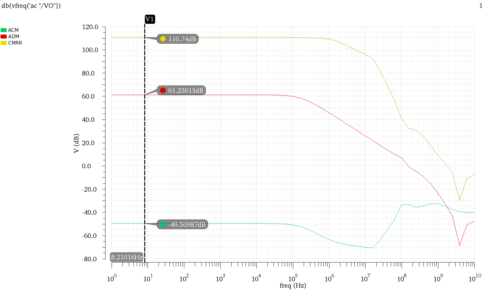
CMRR: 110.74dB
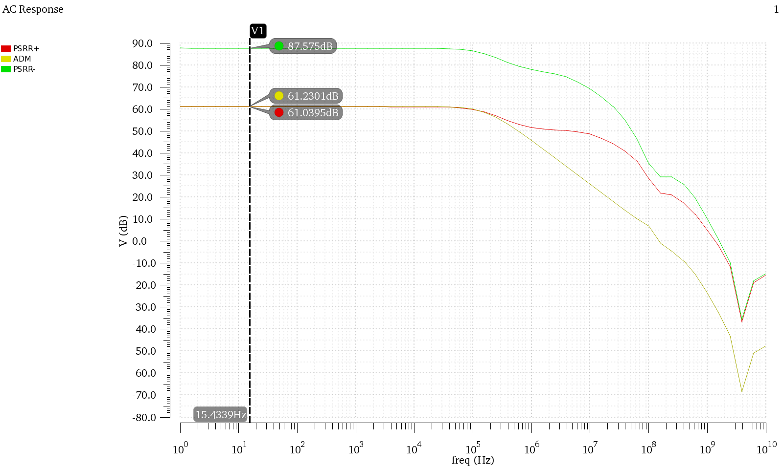
PSRR+: 61.04dB
PSRR-: 87.57dB
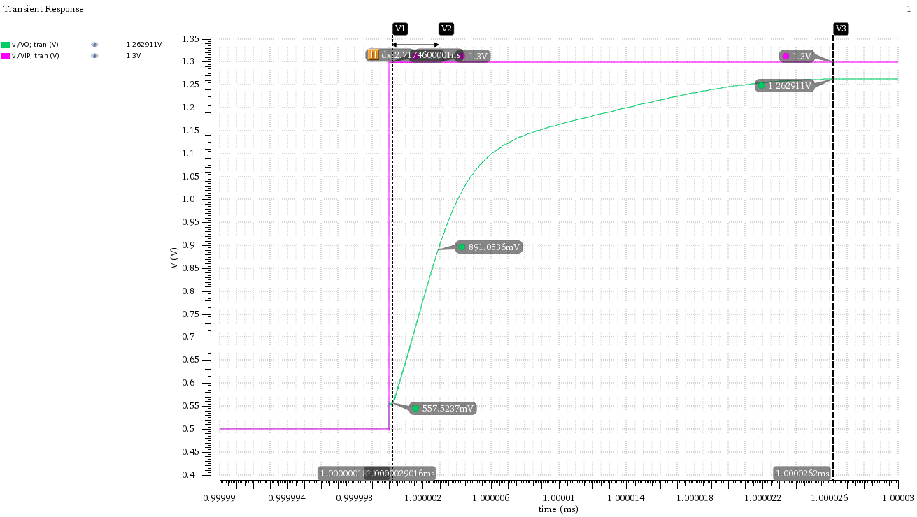
Slew Rate+: 123V/us
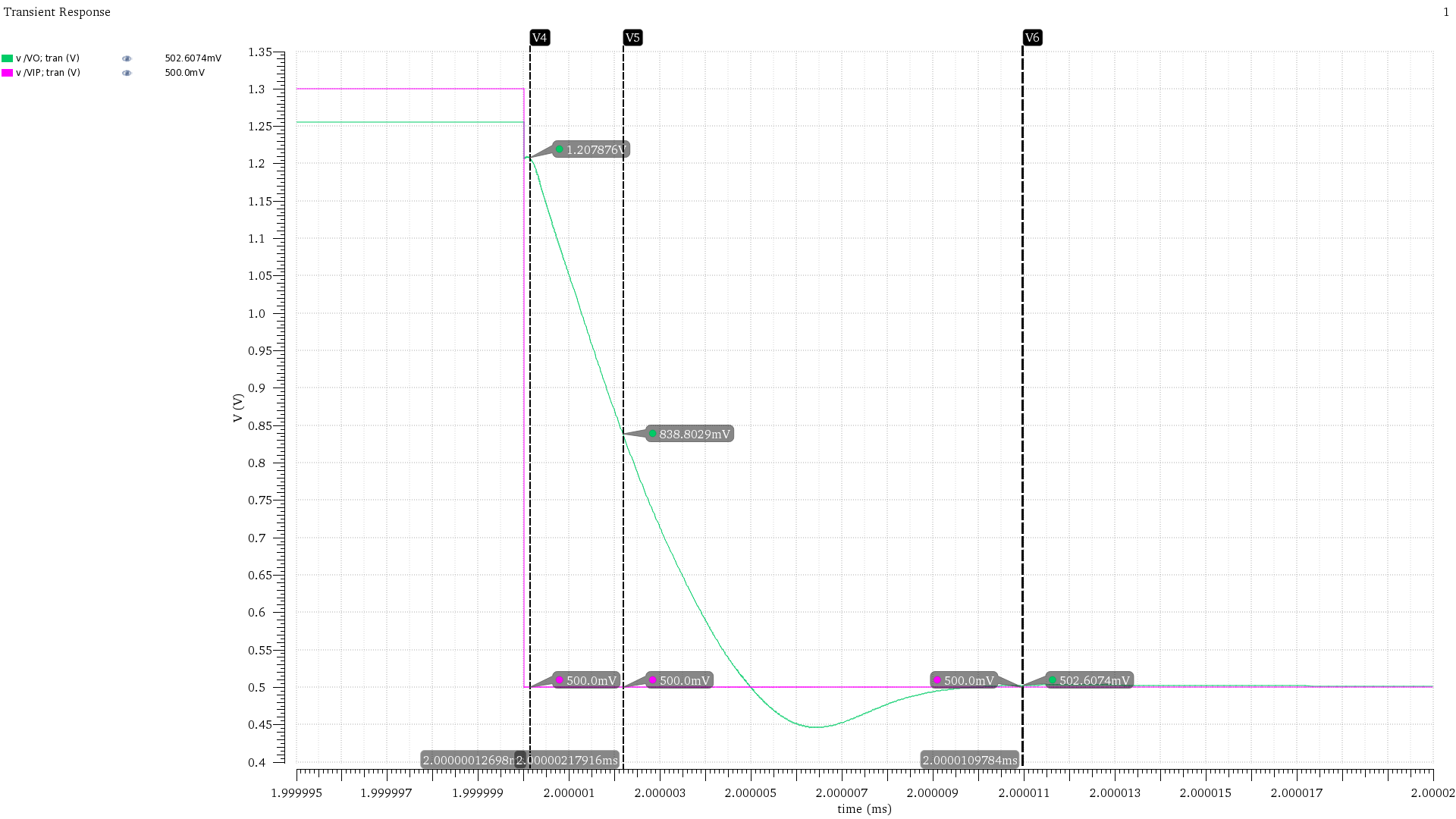
Slew Rate-: 408 V/us
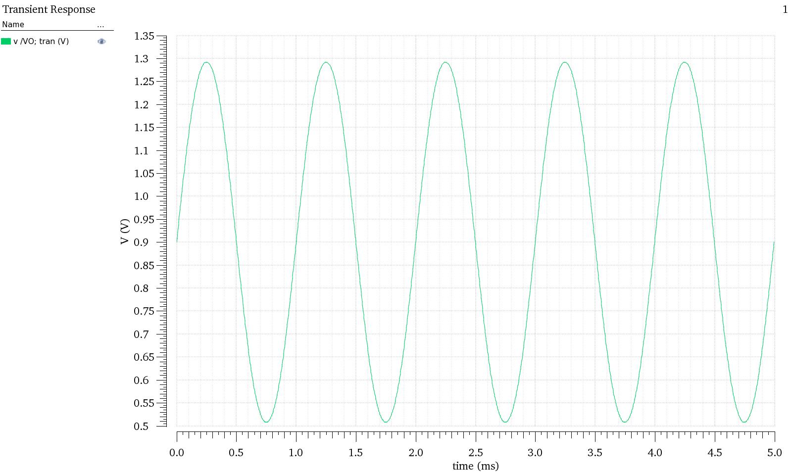
Output Swing: 0.5~1.3V
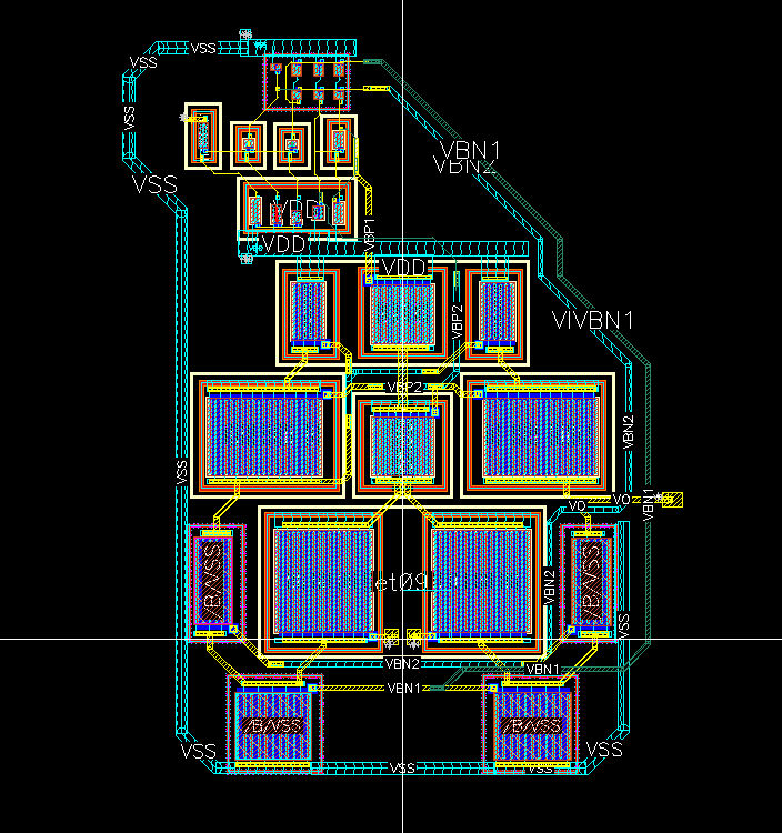
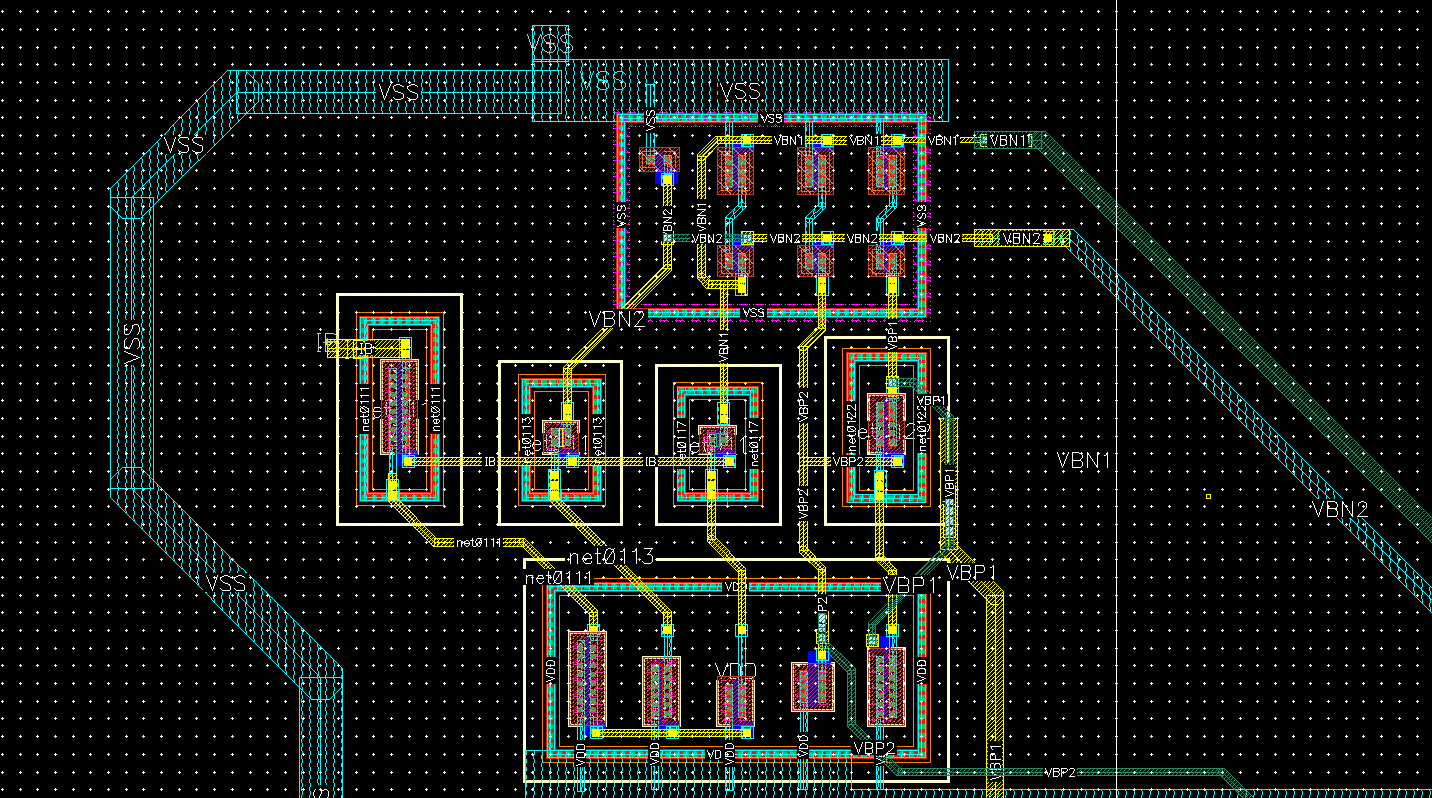
Layout
Layout (Bias Circuit)
The End
deck
By aic999