Transistors
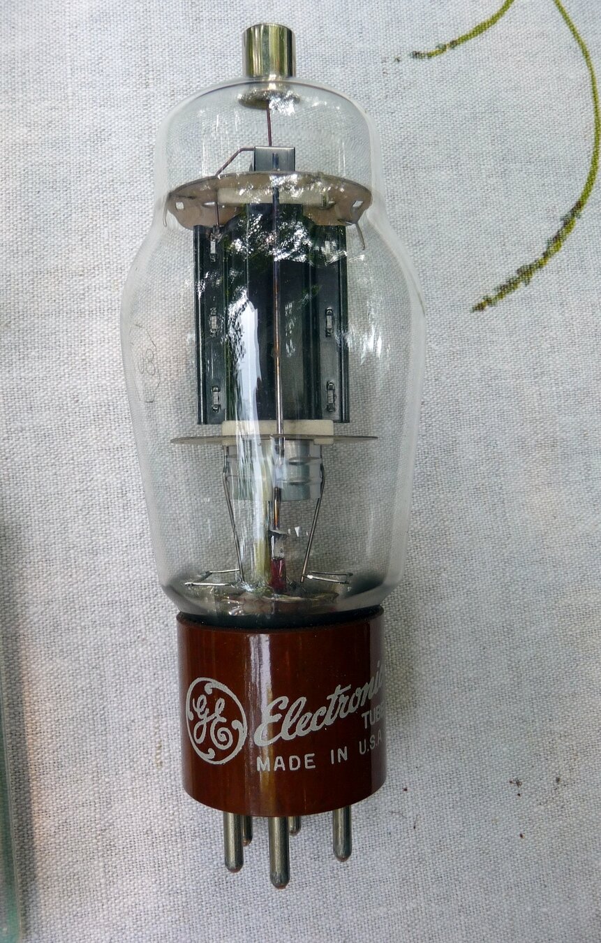
OLD TRANSISTORS: VACUUM TUBES
BIPOLAR JUNCTION TRANSISTORS: PNP and NPN
N-Type
P-Type
N-Type
P-Type
N-Type
P-Type
Emitter
Base
Emitter
Base
Collector
Collector
PNP
NPN
BJT TRANSISTORS: Parameters
w_B
Emitter
Base
Collector
N_{A,E} \approx10^{18}-10^{20}
N_{A,C} \approx 10^{14}-10^{16}
N_{D,B} \approx 10^{16}-10^{18}
\begin{cases}
w_B \leq L_p \approx 50 \mu m\\
N_{A,E} \gg N_{A,B} > N_{A,C}
\end{cases}
Geometrical and doping conditions
BJT TRANSISTORS: Operation Modes
Emitter
Base
Collector
Emitter
Base
Collector
Emitter
Base
Collector
Emitter
Base
Collector
Forward Active
Reverse Active
Saturation
Cutoff
-
EB: Forward bias
-
BC: Reverse Bias
-
EB: Reverse bias
-
BC: Forward Bias
-
EB: Forward bias
-
BC: Forward Bias
-
EB: Reverse bias
-
BC: Reverse Bias
+ -
+ -
- +
- +
+ -
- +
- +
+ -
BJT PNP TRANSISTOR: Forwad Active Mode
Emitter
Base
Collector
+ -
+ -
I_E
I_C
I_B
\begin{cases}
I_{E} = I_{B} + I_{C} \\
I_{C} = \beta I_{B} \\
I_{C} = \alpha I_{E} \\
\beta \gg 1 \approx 100-1000 \\
\alpha \approx 1
\end{cases}
\beta = \mathrm{Gain}
Electrons
Holes
Diffusion
Drift
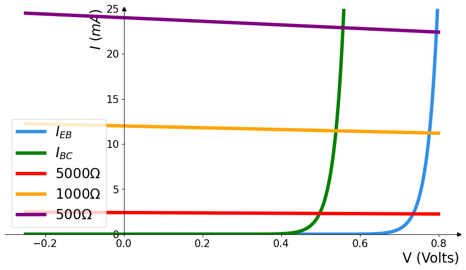
FORWARD ACTIVE MODE: Current Magnitudes and Relationships
p_n(x=0)
Emitter
Base
Collector
\begin{cases}
\\
\\
\\
\end{cases}
p_n(x)
\begin{cases}
J_{D,p}=e D_p \frac{d p_n(x)}{d x} \\[3pt]
\frac{d p_n(x)}{d x} = \frac{\Delta p_n(x)}{\Delta x} = \frac{p_n(x=0)}{w_{B}} \\[3pt]
p_n(x=0) = p_{n0} e^{\frac{e V_{ext}}{k_B T}} \\[3pt]
p_{n0} = \frac{n_i^2}{N_D}
\end{cases}\\
\Downarrow\\
J_{D,p} \approx e D_p \frac{n_i^2}{N_D w_{B}} e^{\frac{e V_{ext}}{k_B T}}
w_B
J_{D,n}=e D_n \frac{d n_p(x)}{d x} = e D_n \frac{d \Delta n_p(x)}{d x} \\[5pt]
\Downarrow\\[3pt]
J_{D,n}=\frac{e D_n}{L_n} \Delta p_n(0)=\frac{e D_n}{L_n}\left(n_p(0)-n_{p 0}\right) \\
J_{D,n}=\frac{e D_n n_{p 0}}{L_n}\left[\exp \left(\frac{e V}{k_B T}\right)-1\right] \\
\Downarrow\\[3pt]
J_{D,n} \approx \frac{e D_n n_i^2}{L_n N_A} e^{\frac{e V_{ext}}{k_B T}}
Hole Current Density
Electron Current Density
\frac{J_{D,p}}{J_{D,n}} \approx \frac{I_C}{I_B} \propto \frac{N_{A,E}}{N_{D,B}} \approx \beta
PRACTICAL CIRCUITS: Current flowing through a loaded PN junction
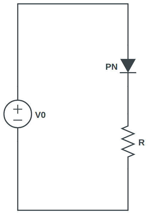
\begin{cases}
I_{PN}=I_{s 0}\left[\exp \left(\frac{e V_{PN}}{k_B T}\right)-1\right] \\
I_{R} R + V_{PN} = V_{0} \\
I_{R} = I_{PN}
\end{cases}
\Rightarrow
I_{R} = \frac{V_{0}}{R} - \frac{V_{PN}}{R} \\
\Downarrow \\
V_{PN} \approx 0.7V
PRACTICAL CIRCUITS: Common Emitter Amplifier


Common Emitter
Thevenin Equivalent
V\(_{0}\)=10V
V\(_{0}\)=10V
V\(_{B}\)=5 V
Copy of Materials and Platforms for AI - Transistors
By Giovanni Pellegrini


