NAND to MIPS
A Crash Course in CPU Architecture
Alex Skryl
@_skryl_
MIPS
Used to stand for Microprocessor without Interlocked Pipeline Stages.
It is a RISC (Reduced Instruction Set Computer) ISA.
An ISA (Instruction Set Architecture) is a specification for the set of opcodes implemented by a particular CPU architecture.
RISC
Has nothing to do with the number of instructions.
Amount of work that an instruction performs is "reduced".
Most instructions are of uniform length and similar structure.
These properties will prove helpful when we construct a MIPS processor.
Assemblers
Converts assembly code to machine code.
The Architecture Instruction Set determines the available operations and binary format.
Automatically calculates code offsets and jump locations using labels.
Sometimes adds sugar like includes, macros, etc.
ASSEMBLY EXAMPLE
Add/Sub: |--op[6]--|--rs[5]--|--rt[5]--|--rd[5]--|--shamt[5]--|--funct[6]--|Beq: |--op[6]--|--rs[5]--|--rt[5]--|--immediate[16]--|Lw/Sw: |--op[6]--|--rs[5]--|--rt[5]--|--immediate[16]--|
  0. add r9,r5,r1
  1. sub r9,r9,r6
  2. beq r9,r0,-8
  3. lw  r1,100(r2)
  4. sw  r9,100(r2)

  0. 000000 00111 00001 01001 00000 100000  [ 0 5 1 9 0 32 ]
  1. 000000 01001 00110 01001 00000 100010  [ 0 9 6 9 0 34 ]
  2. 000100 01001 00000 11111 11111 111110  [ 4 9 0   (-2) ]
  3. 100011 00010 00001 00000 00001 100100  [ 35 2 1 (100) ]
  4. 101011 00010 01001 00000 00001 100100  [ 43 2 9 (100) ]
Digital Systems
Digital means discrete. Electrical values are treated as integers, normally 0 (low voltage) and 1 (high voltage) as opposed to real numbers (analog).
The assumption that at any time all signals are either 1 or 0 hides a great deal of engineering.
We will ignore all issues of electrical engineering and assume square waves.
Combinatorial circuits
Do NOT have memory elements.
Do NOT have loops (topological ones).
Output is dependent only on inputs and NOT on any pre-existing state.
Simply a mathematical function from inputs to outputs.
Truth tables are a convenient way to represent the input/output mappings for these functions.
sequential circuits
Contain memory/state.
Output depends on input AND state.
Can have toplogical loops.
boolean algebra
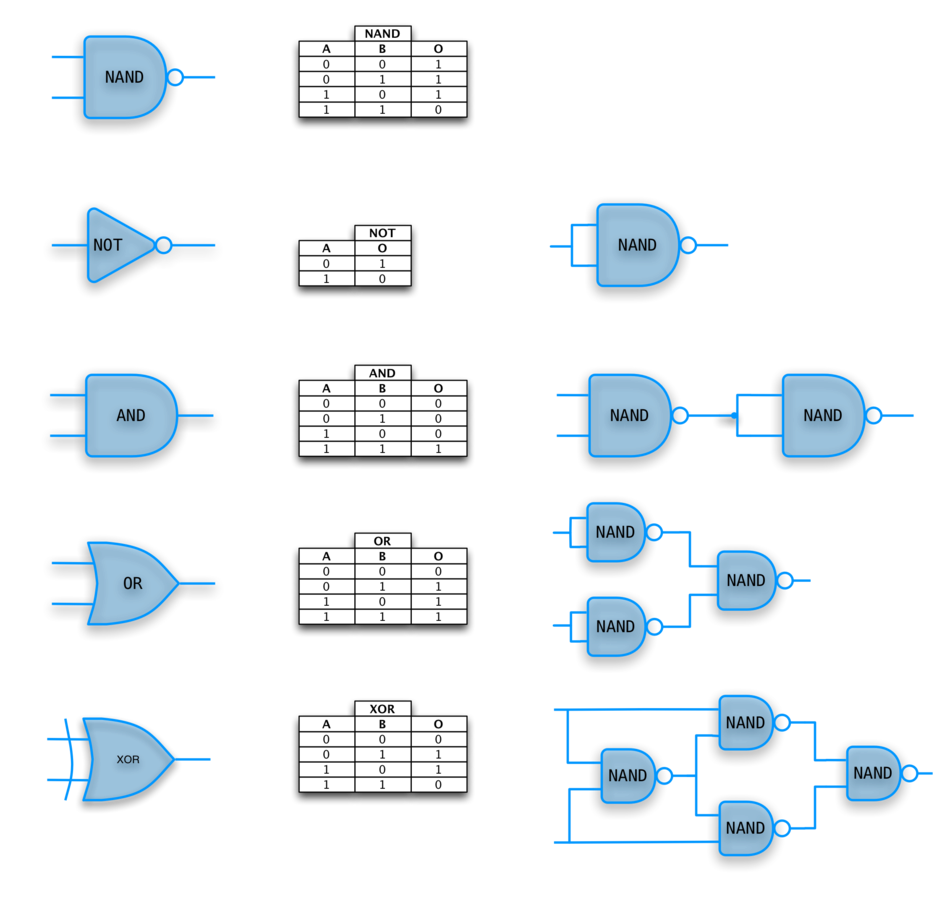
Primary operations are the conjunction AND, disjunction OR, and negation NOT.
All boolean functions can be represented using these three operations. Together, these three operations are universal.
Both NAND and NOR are also universal (can be used on their own to implement and, or, not)
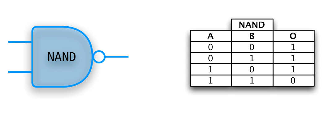
NAND
NAND Universality
CNF
Stands for Conjunctive Normal Form.
Arbitrary boolean functions can be represented as a sum of products given their truth table.
XOR can be described as A'B + AB'
DeMORGAN's Laws
not (A and B) is the same as (not A) or (not B)
not (A or B) is the same as (not A) and (not B)

COMBINATIOnal logic
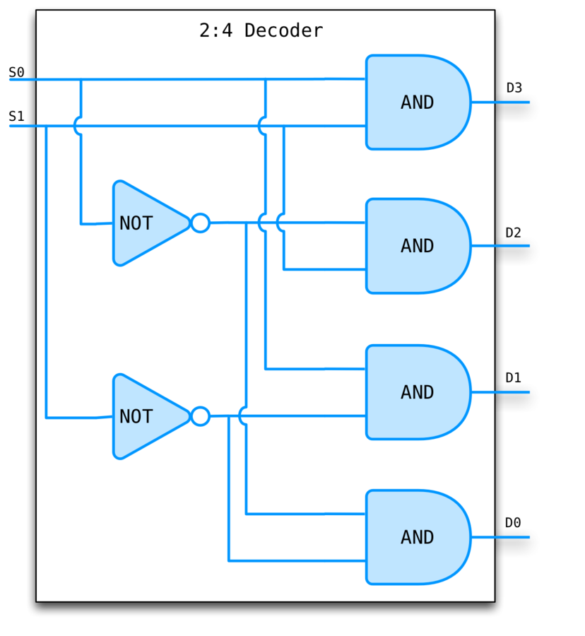
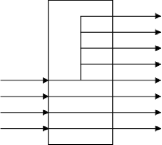
DECODERS
Converts an n bit signal to a 2^n bit signal with a single line set to true.
The encoded form takes fewer bits so is better for communication.
The decoded form is easier to work with. For example, to check if something is a 5 just test the fifth wire...
Encoders perform the reverse operation.
DECODER EXAMPLE
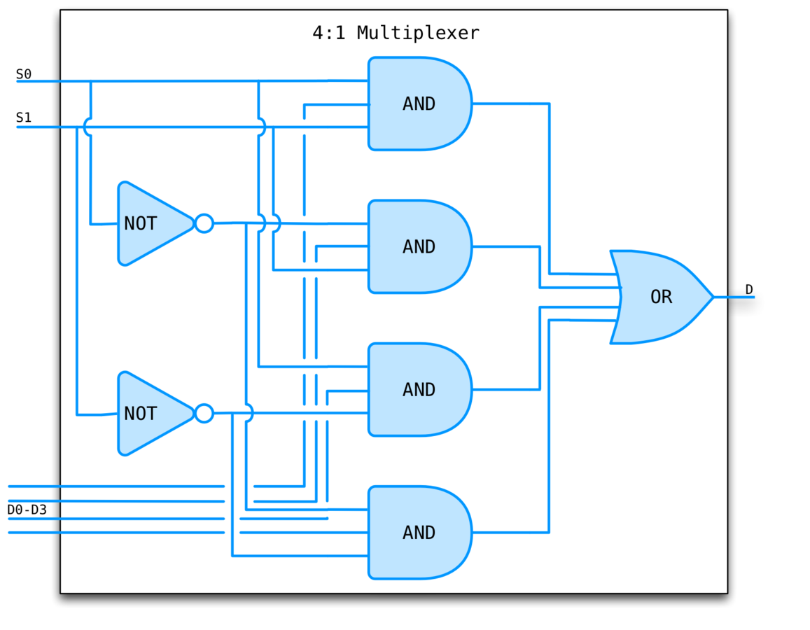
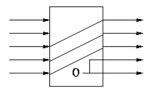
MULTIPLEXeR
Often just mux.
Used to select one output signal from a group of input signals based on the value of the select lines.
A multiplexer of 2^n inputs has n select lines.
A demultiplexer performs the inverse operation.
MUX EXAMPLE
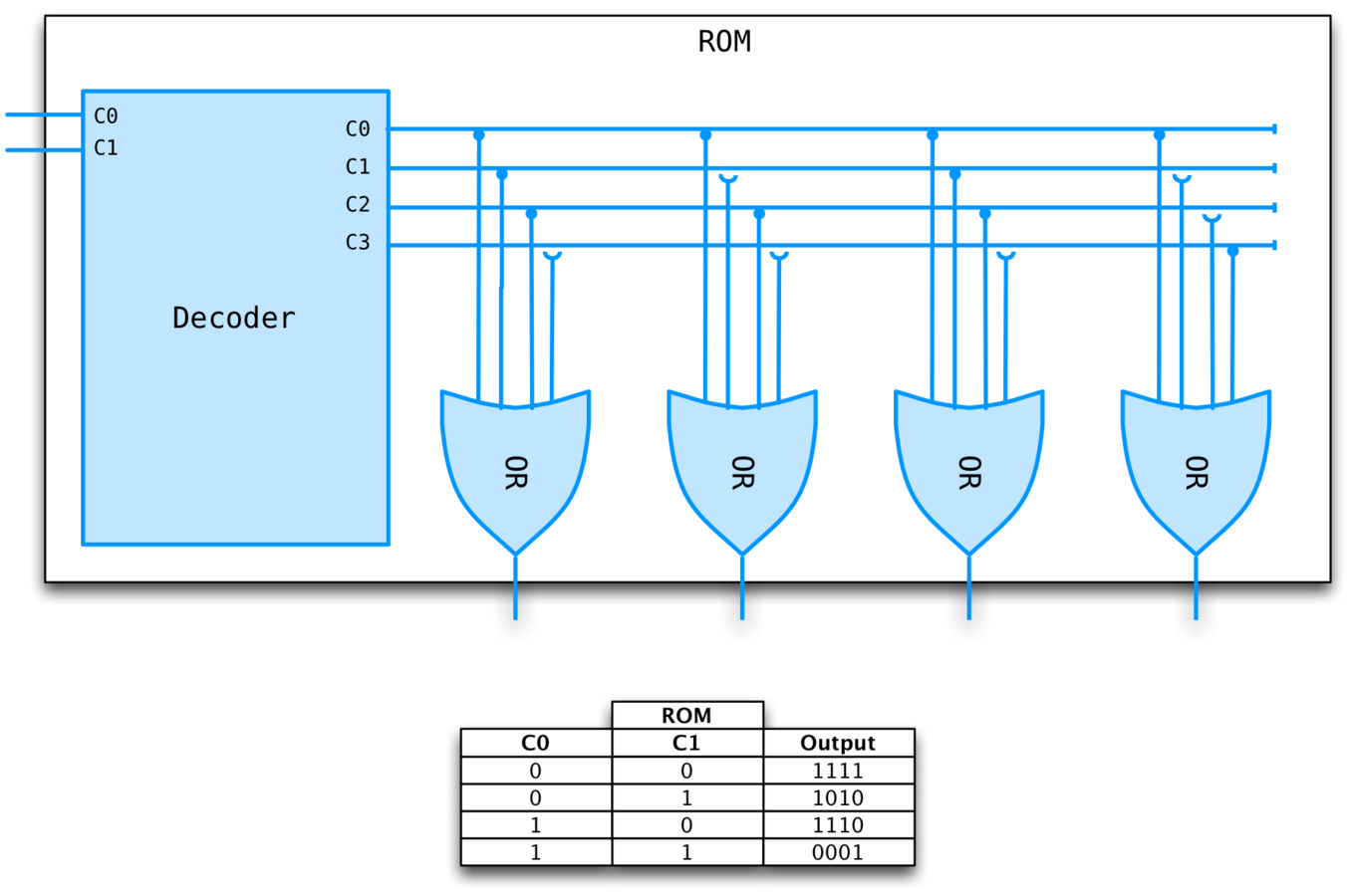
ROM
Stands for Read Only Memory.
It does NOT have state and can be implemented using a combinational circuit with a 1-1 mapping from inputs to outputs.
Essentially a lookup table. Given an address, produces the value stored at that address.
ROM EXAMPLE
MATH
2s complement
We need to represent negative numbers in binary. How? Format wars!
1s complement (bit inversion) is inconvenient because there are two representations of 0 (ex. 0000 and 1111) as well as other reasons.
2s complement is 1s complement + 1, makes arithmetic very easy.
-0000 = 1111 + 1 = 0000 (only one 0)-0001 = 1110 + 1 = 1111(1 + -1) = 0001 + 1111 = 0000
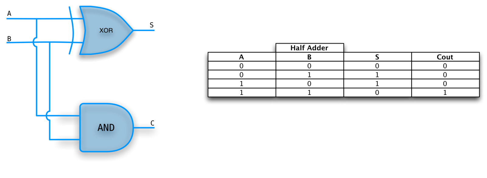
HALF ADDER
A 1-bit adder with no carry in. Doesn't scale!
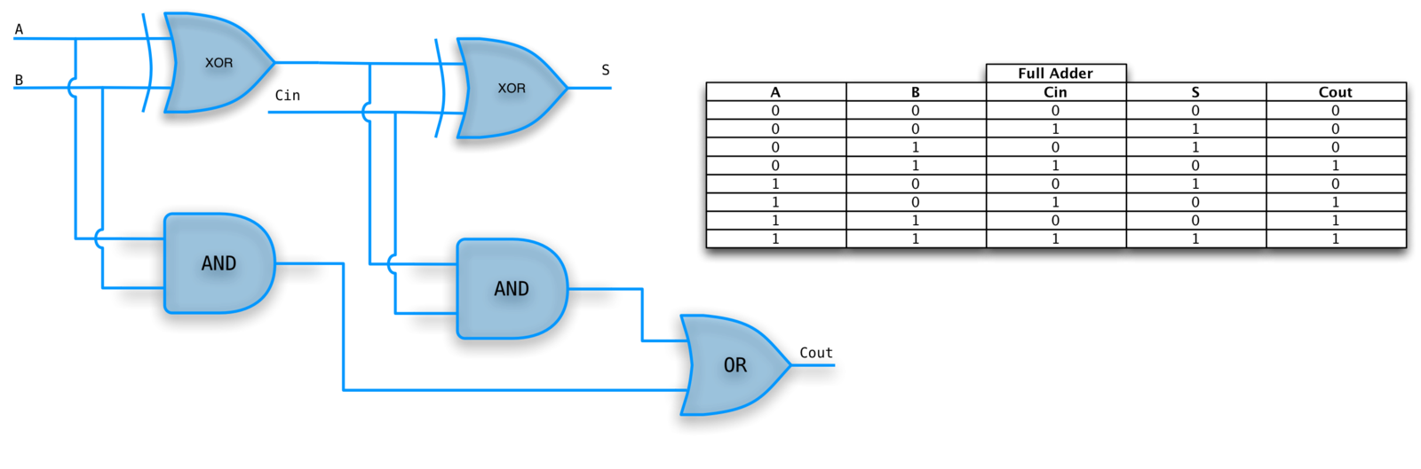
Full adder
We need a carry in if we want to create multi-bit adders.
Three 1-bit inputs, X, Y, and CarryIn.
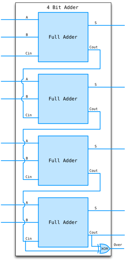
4bit adder
Linear time complexity since carry bit must ripple through all adders.
For better performance see Carry Lookahead Adders.
An overflow occurs when the carry in for the HOB does not equal its carry out. Why?
Case 1: 0 carried in, 1 carried out. Only way a 1 can be carried out is if both HOBs are 1. This is the case when you add two negative numbers, but the result is positive.
Case 2: 1 carried in, 0 carried out. Only way a 0 can be carried out is if both HOBs are 0. This is the case where you add two positive numbers and get a negative result.
Case 2: 1 carried in, 0 carried out. Only way a 0 can be carried out is if both HOBs are 0. This is the case where you add two positive numbers and get a negative result.
4bit adder example
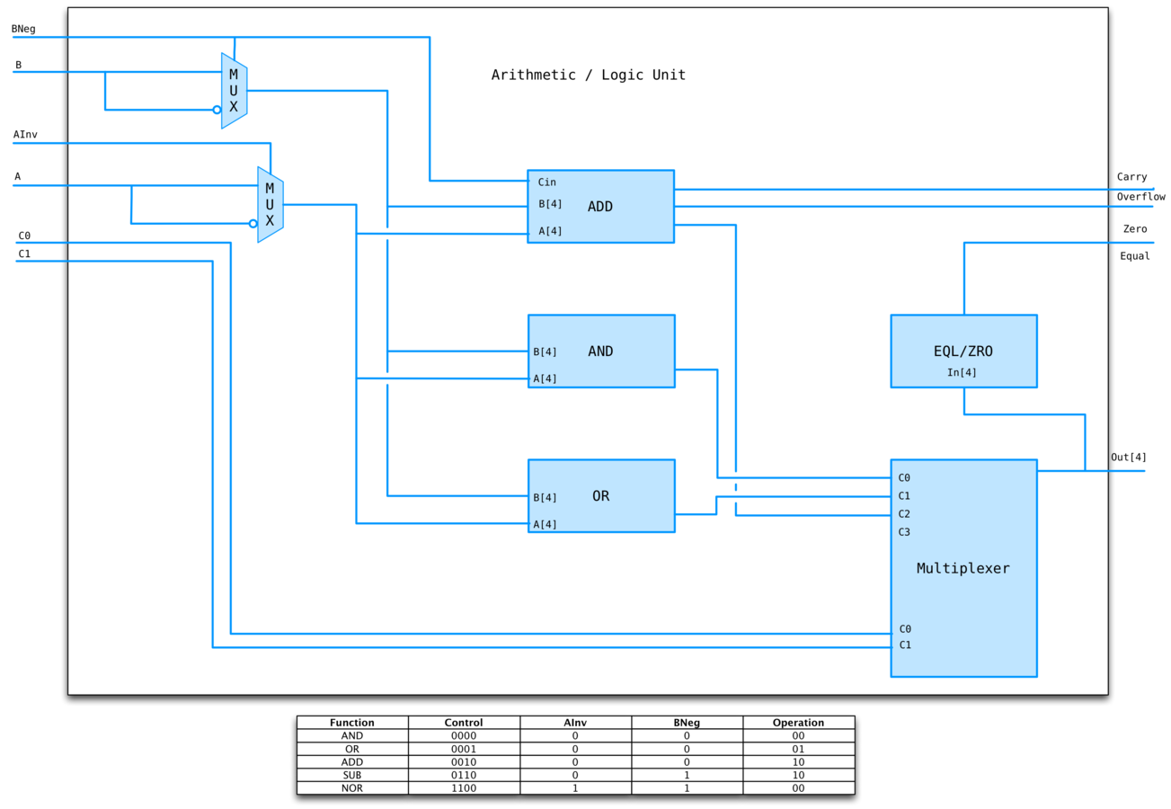
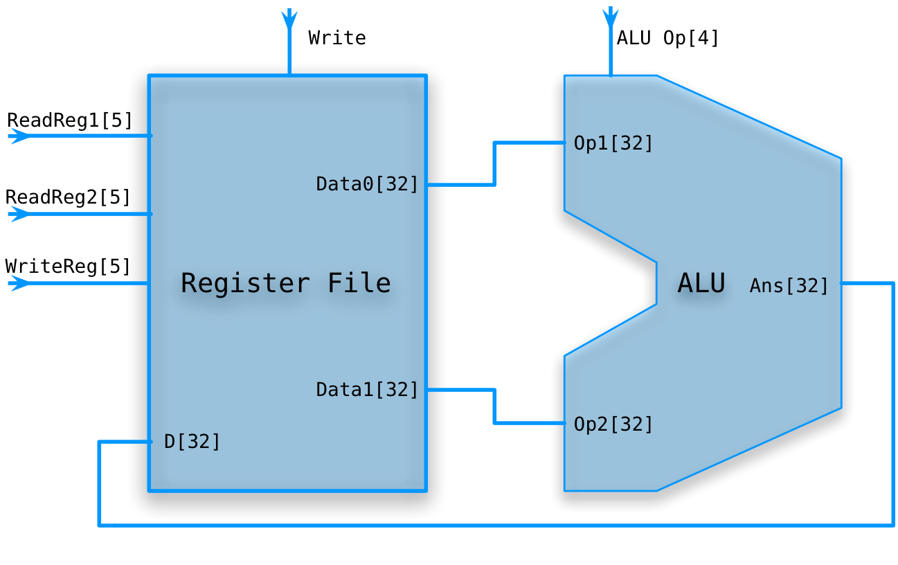
ALU
We can combine multiple math operations using a result MUX.
To subtract, convert first input to it's 2s complement and add. To convert to 2s complement, invert and set Cin.
Multiply instructions only started showing up in the early 80s, prior to that it was implemented as a subroutine. We'll ignore these.
MIPS has NOR but that's just (A + B)' = A'B', so we can invert both inputs and reuse AND, voila!
ALU EXAMPLE
Memory and State
synchronous systems
State elements have a clock as an input and only change state at the active edge of the clock.
All signals written to the state element must be valid at the time of the active edge.
If cycle time is 10ns, the combinational logic that computes the input to a state element must have settled on the correct output within 10ns.
CLOCK EXAMPLE

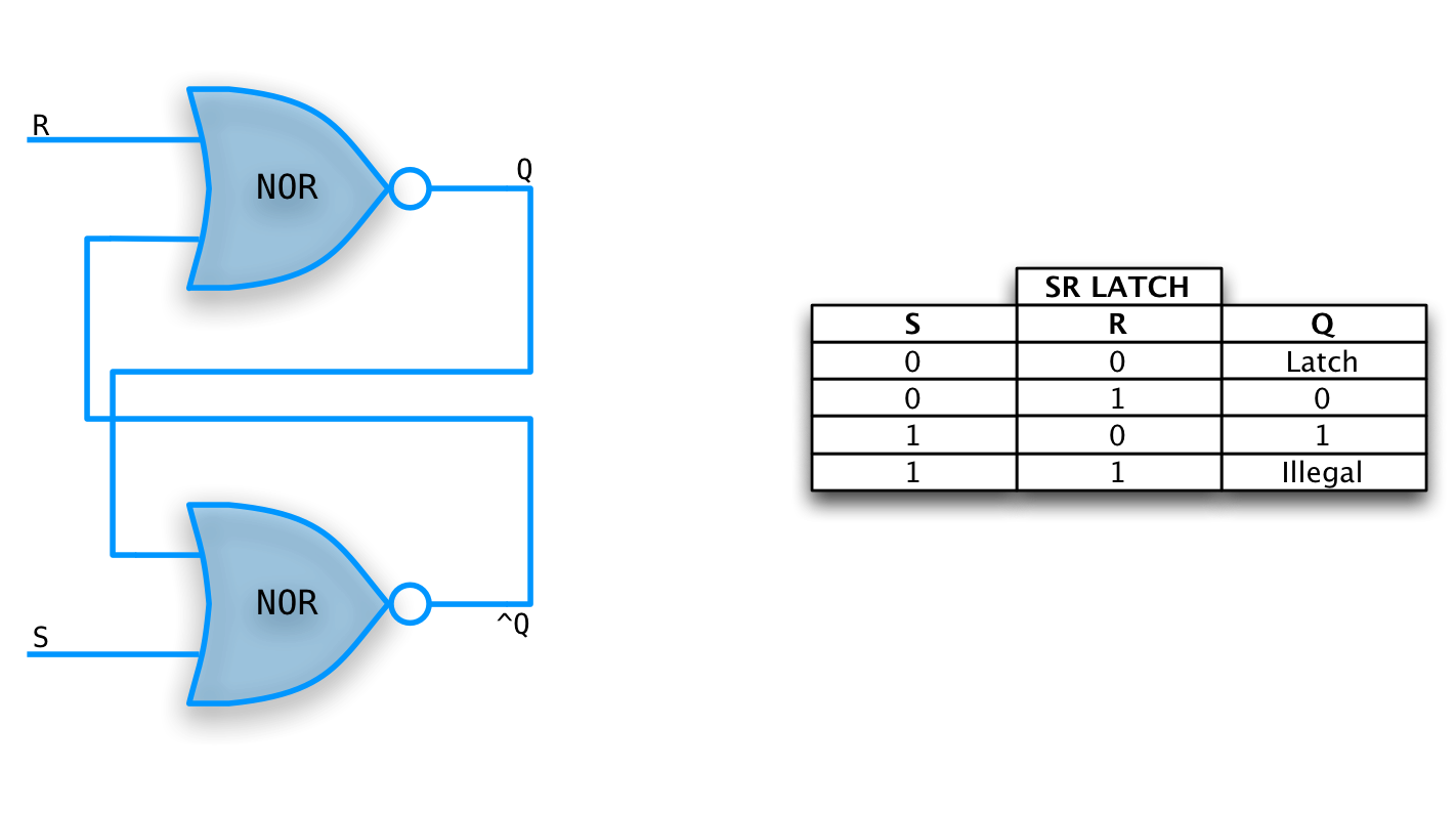
S-R Latch
A simple, un-clocked memory element.
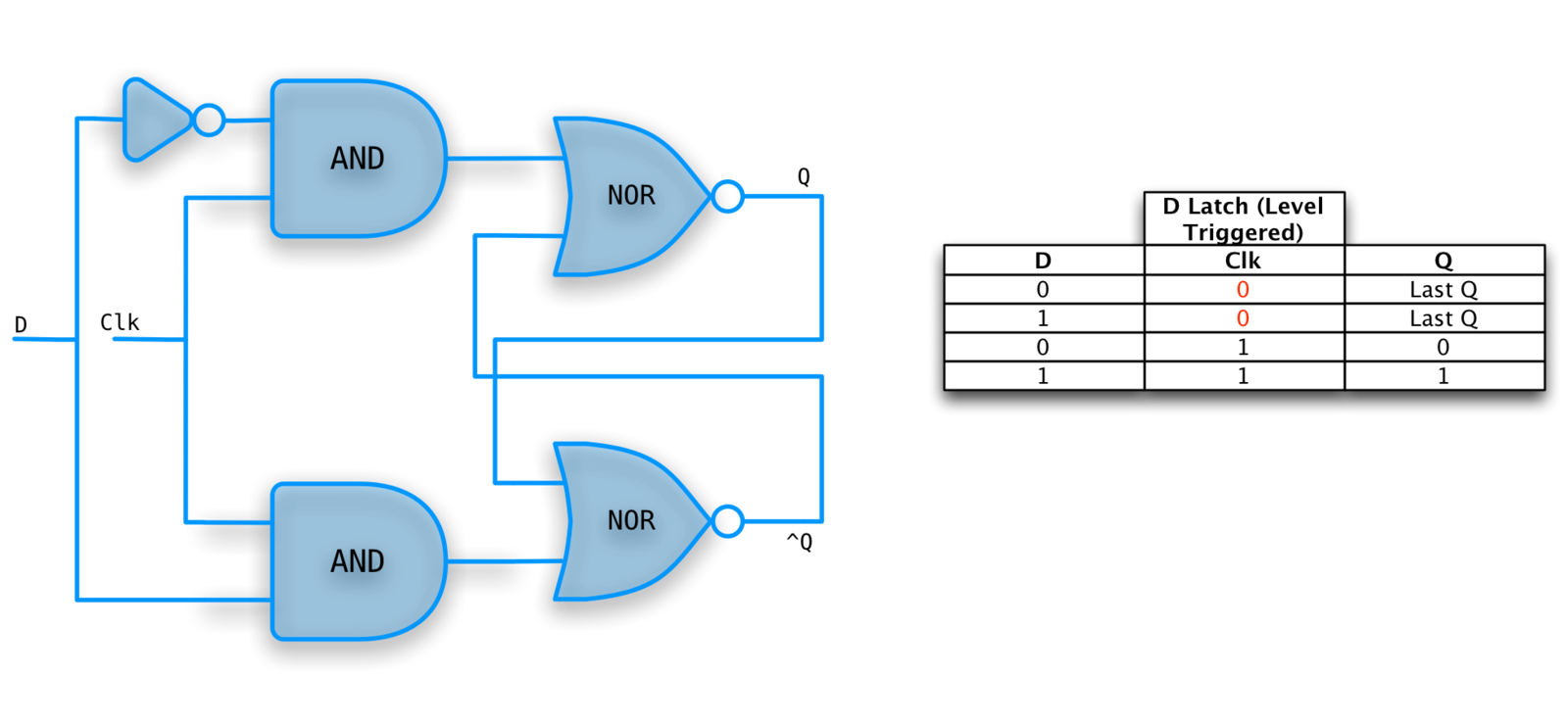
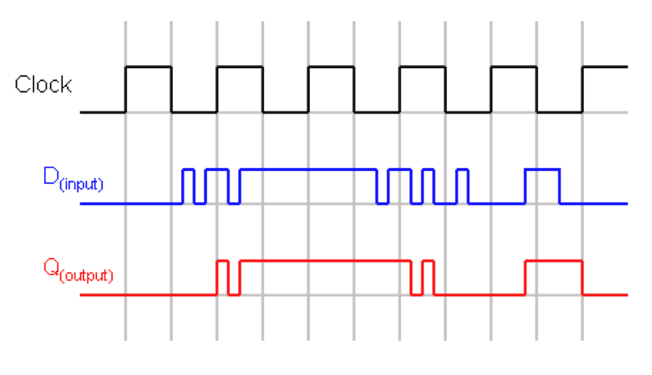
D-Latch
D is for Data.
Right part is just an S-R Latch.
Left part changes the interface to a data line and a clock.
When clock is high, latch is transparent (output equals input).
D-LATCH example
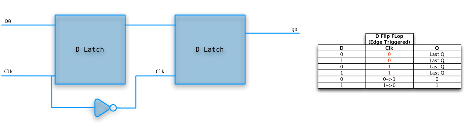
D-Flip Flop
Also called Master-Slave Flip Flop.
An edge triggered, clocked memory. This is what we want!
Built from two D-latches which are transparent. The flop however is not.
Changes to the output occur only at the active edge.
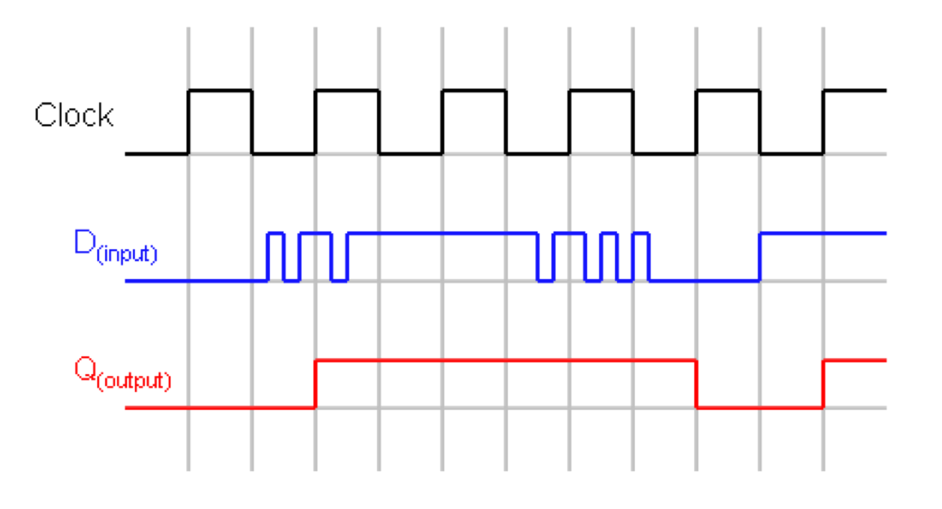
D-Flop example
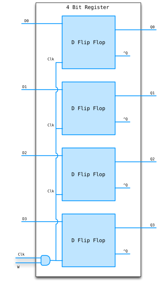
Registers
An array of D-flip flops.
What if we don't want to write the register during a particular cycle? Need to add a write line.
REGISTER EXAMPLE
Register file
A set of numbered registers.
To access, simply supply the register number, the write line, and, if write is asserted, the data to be written.
You can read and write the same register during one cycle. Read the old value and replace it at the end of the cycle.
Can have multiple read and write ports. Ours will have 2 read, 1 write.
Register file example
A Reduced MIPS ISA
R-Type instructions
These instructions have three operands, each is a register number.
|---op[6]---|---rs[5]---|---rt[5]---|---rd[5]---|---shamt[5]---|---funct[6]---| -
op - op code
-
rs, rt - source registers
-
rd - destination register
-
shamt - shift amount
-
funct - used for op 0 to distinguish ALU operations
Add and Subtract
Also and, or, nor (not is special case of nor)
add/sub $9,$10,$11
|000000|01010|01011|01001|00000|100000| Register 9 becomes register 10 + register 11.
-
op=0, signifying an alu op.
-
The shamt is not used (set to zero).
-
funct=32 specifies add to the ALU.
-
Do sub by just changing the funct.
Jump register
jr $31
|000000|11111|00000|00000|00000|001000|
Jump to the location in register 31.
An R-type instruction, but uses only one source register rs.
I-TYPE INSTRUCTIONS
These instructions have an immediate third operand, i.e., the third operand is contained in the instruction itself.
|---op[6]---|---rs[5]---|---rt[5]---|---immediate[16]---|
The instruction specifies two registers and one immediate operand.
-
rs is a source register.
-
rt is sometimes a source and sometimes a destination register.
Load/store word
lw/sw $9,1000($19)
|100011|10011|01001|0000001111101000|
$9 is loaded with the contents of Mem[$19+1000].
- The constant 1000 is the immediate operand.
- These instructions transfer a word (32 bits) from/to memory.
- But the machine is byte addressable! What if the memory address is not a multiple of 4? An error (MIPS requires aligned accesses).
ADD IMMEDIATE
addi $9,$10,100
|001000|01010|01001|0000000001100100|
The effect of the instruction is $9 = $10 + 100
The immediate operand in addi can be negative to perform subtraction.
BRANCH equal/not equal
beq/bne $9,$10,123
|000010|01010|01001|0000000001111011|
if reg9 == reg10 then go to the 124th instruction after this one.
Why 124 not 123? We will see that the CPU adds 4 to the program counter (for the no branch case) and then adds (4 times) the third operand.
Normally one writes a label for the third operand and the assembler calculates the offset needed.
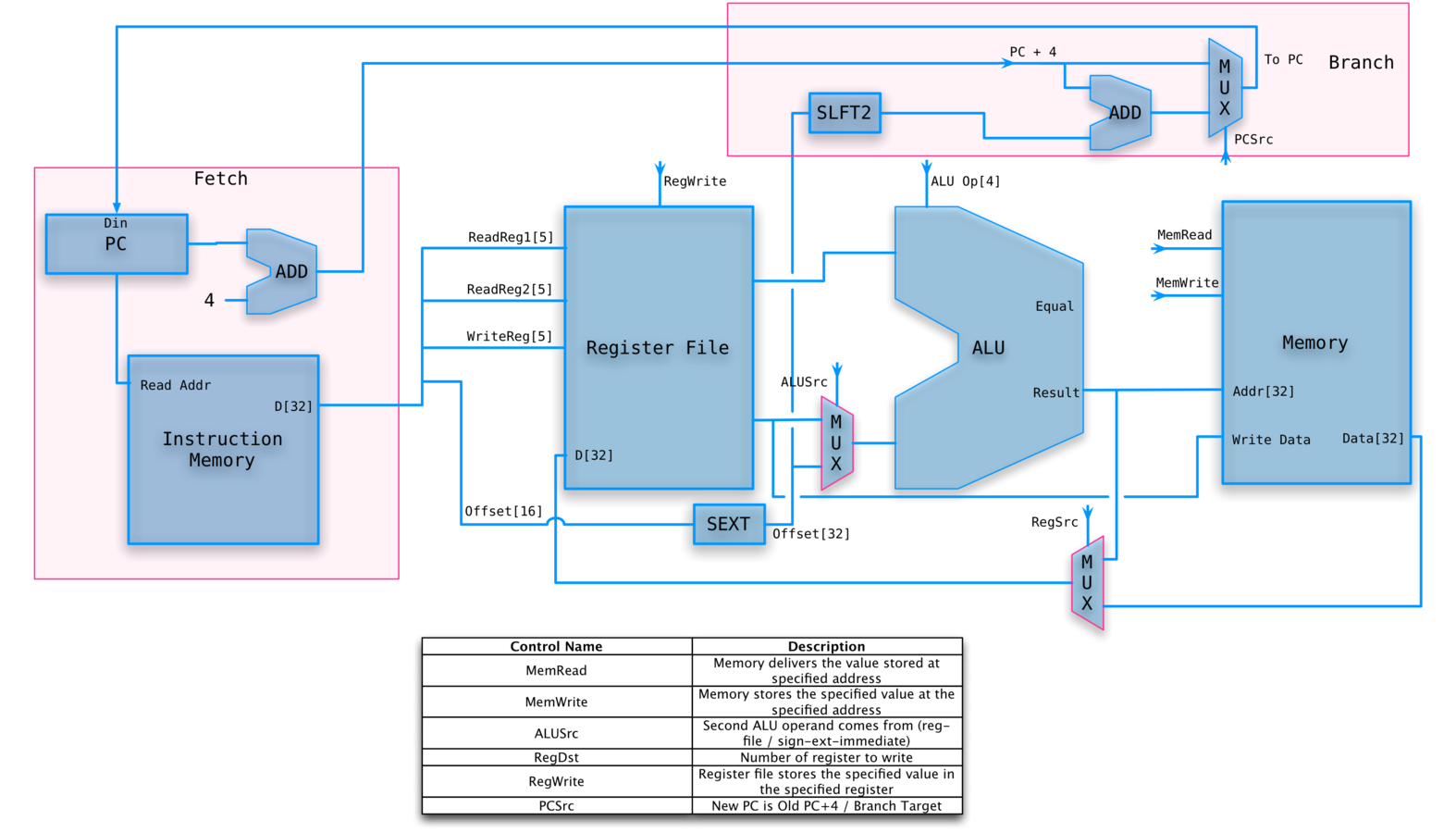
The processor
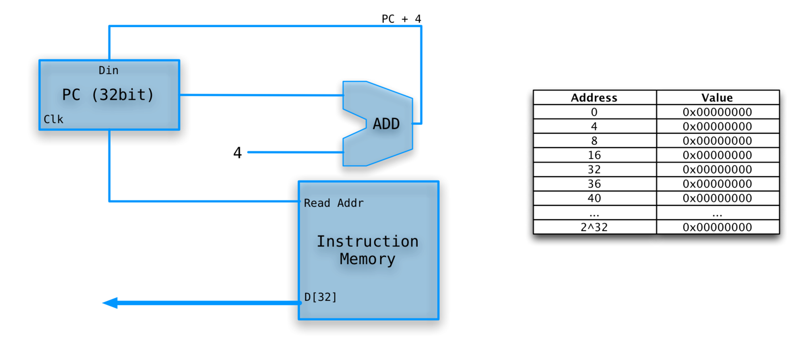
INSTRUCTION FETCH
Ignoring branches and jumps.
PC (Instruction Pointer) register is written every cycle (don't need write line).
Clock lines will not be drawn (I'm lazy).
FETCH EXAMPLE
R-type instructions
add rd,rs,rt
Require two read ports and one write port, that's why we designed our register file that way.
32 bit bus is divided into 5 3-bit buses. Other wires not shown.
R-TYPE PATH
Load/store word
lw/sw rt,disp(rs)
We need to extend the 16 bit immediate constant to 32 bits. That is, we must add 16 more HOBs that match the sign bit of the immediate.
We don't need gates to do this, just wires.
Load/store path
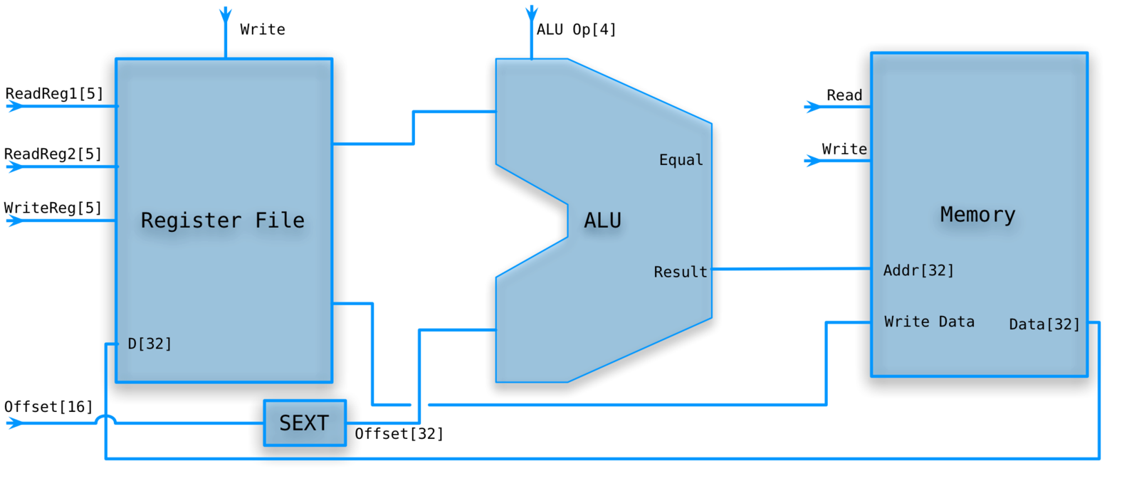
-
RegWrite is deasserted for sw and asserted for lw.
-
MemWrite is asserted for sw and deasserted for lw.
-
Don't really need MemRead for our memory.
-
The ALU op is set to Add.
Branch on equal
beq rs,rt,disp
The constant represents 32 bit words but the address is specified in 8 bit bytes.
Need to convert byte offset to instruction offset by multiplying by 4 (left shift 2).
BRANCH ON EQUAL PATH
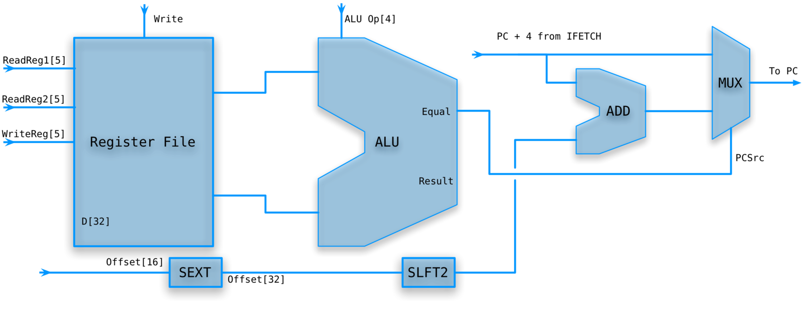
- Set ALU to subtract rs from rt and check equal flag.
-
The target address is the sum of PC (after it has been incremented) and the 16bit immediate constant disp.
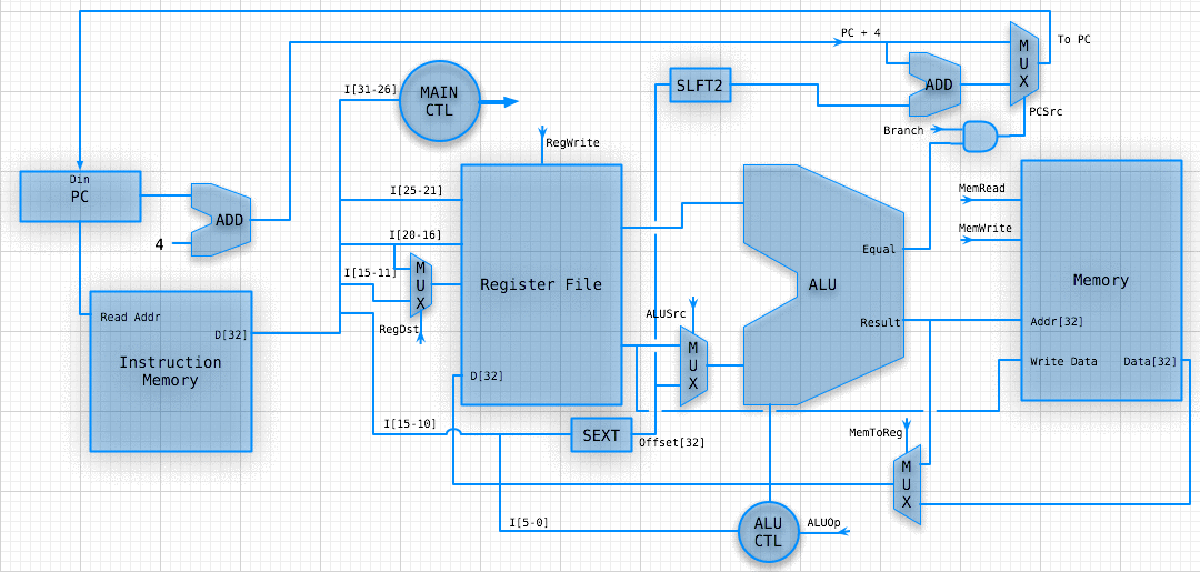
A single datapath
We are assuming that the instruction memory and data memory are separate. So we are not permitting self modifying code.
We are ignoring IO.
Still manual control.
SINGLE DATA PATH
Who runs the show?
We still need to divide the instruction correctly, and add something that will set the control lines.
We will let the main control summarize the opcode for us.
From this summary and the 6-bit funct field, we shall determine the control lines for the ALU.
CONTROLLED PATH
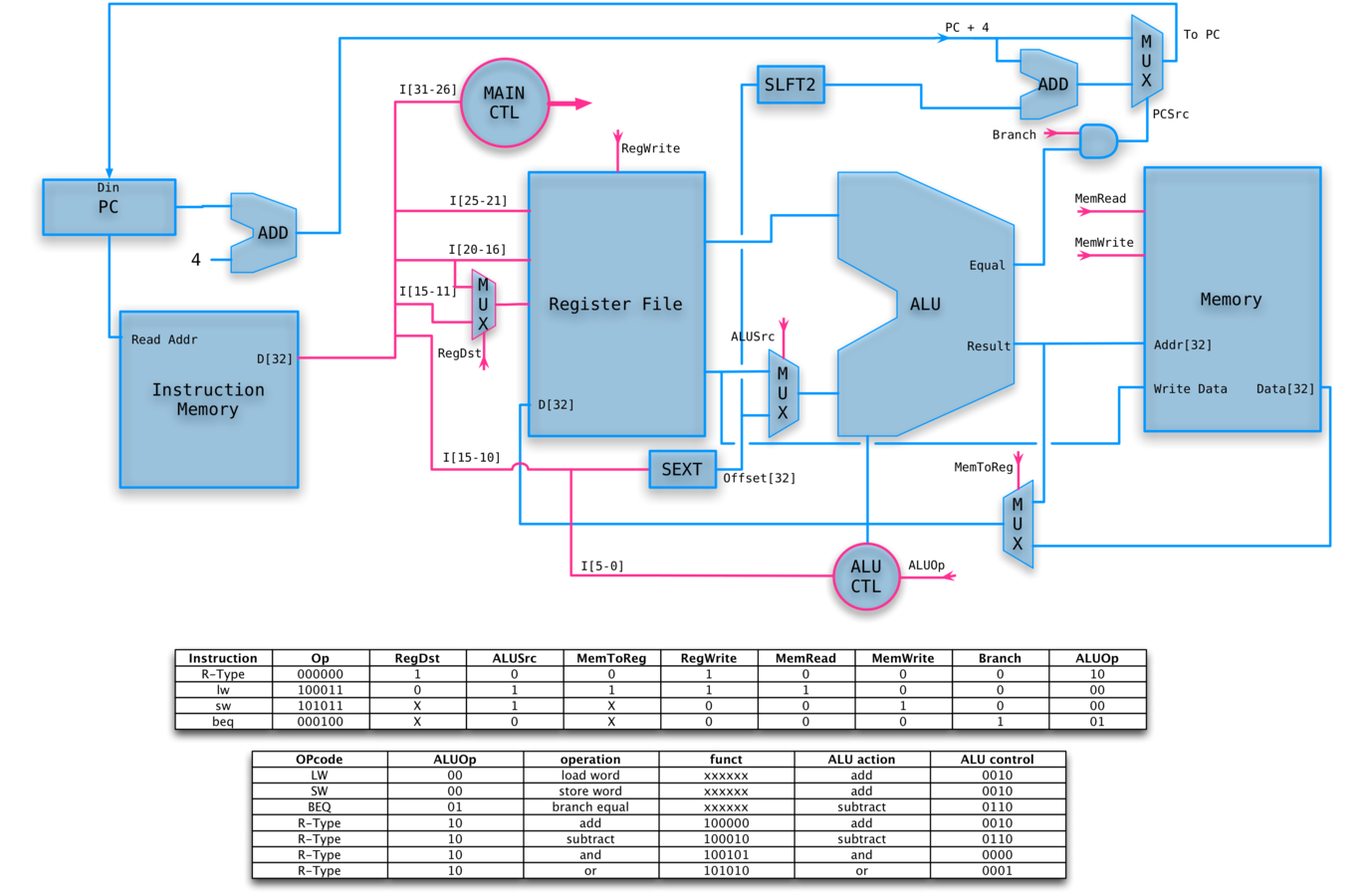
ANIMATED R-TYPE OP
WHY DOES THIS SUCK?
Some instructions are likely slower than others and we must set the clock cycle time long enough for the slowest.
The disparity between the cycle times needed for different instructions is quite significant when one considers implementing more difficult instructions, like divide and floating point ops.
Actually, if we considered cache misses, which result in references to external DRAM, the cycle time ratios would exceed 100.
possible solutions
Variable length cycle.
Multi-cycle instructions.
Pipelined cycles.
Multiple data paths (superscalar).
VLIW (Very Long Instruction Word).
references
NAND to MIPS
By Alex Skryl
NAND to MIPS
A crash course in computer architecture.
