Gaining RF Knowledge:
An Analog Engineer Dives Into RF Circuits
Chris Gammell
Analog Life, LLC
Presented at the Hackaday Superconference 2019
Goals for this talk
- Explain how I entered the world of working with RF
- Explain it without burying you in math
- Give you some resources to make your own way
Who are you?
Electronics experience?
RF experience?
Ham radio experience?
You may have more experience I do!
I wanted this talk to help shortcut some of the struggles I had (and have) when I was getting started with the field of RF.
Who am I?
Chris Gammell
- 15 years of electronics design.
- Have worked in a couple industries
- Semiconductor
- Test and measurement
- Industrial controls
- Component sourcing
- Co-host of The Amp Hour electronics podcast (https://theamphour.com)
- Teaching people electronic design online for the past 5 years as part of Contextual Electronics

Started by working on these

10 PLC = 6 readings per second

Not exactly blazing speed
Higher speed stuff like digital was always there as well, but usually nothing very high speed either (<100 MHz)
So what changed?
RF is everywhere
Every product, that is
RF is everywhere AND in every product

I'm currently designing a product that has 5 antennas on it!
And it's cheap

I assume we have similar goals
You’re interested in making things
You're excited about cheap connected (RF) hardware
And you wonder about how to actually integrate it.
How I got started
I copied the app note
This is actually pretty common
I'd guess at least 80% of most PCB designs are re-implemented app notes
Followed other guidelines in Mike Ossmann's "5 Rules of RF design"
(delivered at Supercon 2015)

https://www.youtube.com/watch?v=TnRn3Kn_aXg
My first RF Design
It worked!

Why?
Why?
- The modem and the antenna were pre-matched
- I minimized my interaction with it (kept the RF trace short)
- Because I didn't need to take it to production
Can we do this all the time?
Maybe!
It depends on your design goals
If you have a completely uncharacterized antenna and source, you are going to have to work a lot harder.
The complexity and level of integration of your circuit will also have a large impact on the likelihood of success.
Reasons I wanted to learn more about RF
Troubleshooting
What happens when things go wrong on the bench?
FCC / CE compliance testing
What happens when things go wrong at the $10K/day test lab?
Being a good RF citizen
Your signals might interfere with someone else's signals and that's not nice.
RF concepts that are tricky
Especially for beginners
We're dealing with things in the frequency domain.
When someone talks about "the spectrum" of a signal
They are asking about the frequency content contained within a signal that exists in the real world.

http://tiny.cc/RigolFFTplot
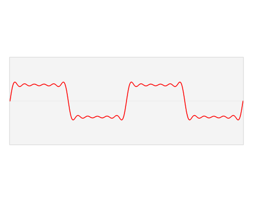
Waterfall Plots
Components act differently based on frequency
- Block frequencies from "passing through" at low frequencies.
- Allow frequencies to "pass through" at high frequencies
- Where this transition happens depends on the capacitance of the component.
Capacitors

- Allow frequencies to "pass through" at low frequencies.
- Block frequencies from "passing through" at high frequencies
- Where this transition happens depends on the inductance of the component.
Inductors
All components have some aspect of inductance and capacitance

Thinking Logarithmically
Logarithmic scales
You're going to see units like "dB", or "dBm" which an easy way to refer to things that change in value by orders of magnitude
As an added bonus: Gains add together
It's all about the power
Most RF circuits deal in power, not in just voltage or current
Analyzing RF subsystems is often about minimizing the degredation of the signal through the system
This is referred to as the "link budget"
What does the RF path look like?

Image courtesy of osmocom.org
We need to ensure all other parts of the system introduce minimal degradation and noise
If a link budget is 100 dB, that means the received signal is 1/10,000,000th as much power as the transmitted signal
Impedance matching ensures we don't introduce signal degradation
Maximum power transfer happens when a source and a load are perfectly matched
A counter example:
What happens when there is a source (like an ESP32) and an antenna (like a PCB antenna) that are not perfectly matched?
Unmatched source and load
-
You won't transmit as far as you thought
-
Your system will be less efficient
-
Energy is "bounced back" and is usually lost to heat or radiated emissions (bad)
-
-
It may not work at all
-
You might damage your output driver section
What is impedance though?
Impedance refers to how a device passes or blocks electromagnetic energy at various frequencies.
Why do we need to do matching at all?
Isn't the antenna designed to work at 50 ohms?
- The world is imperfect!
-
Environmental conditions can affect it, including things like the enclosure or thing surrounding the antenna
-
Antenna manufacturing variations means you might have different specs than stated
Pi network

http://tiny.cc/mo0mbz
"Match a 1000-Ω source to a 100-Ω load at frequency (f) of 50 MHz. You desire a bandwidth (BW) of 6 MHz."
Pi network

http://tiny.cc/mo0mbz
Measurement Tools
(and their measurements)
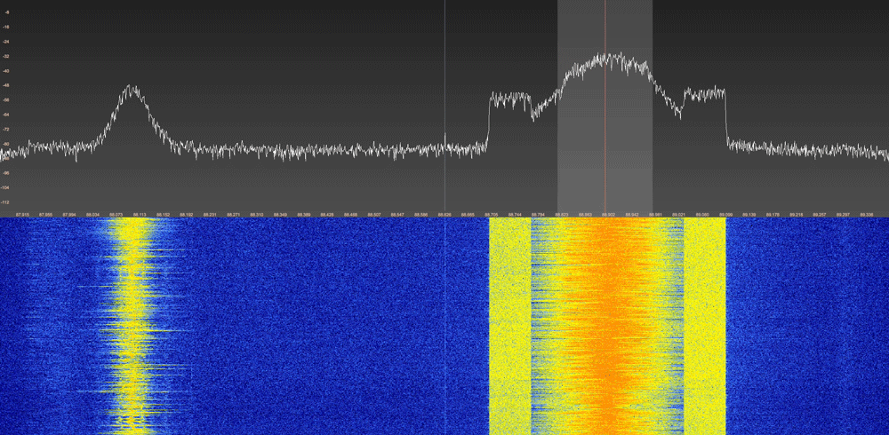
Spectrum Analyzer
Spectrum Analyzer

http://tiny.cc/RigolSA
Spectrum Analyzer
- Allows you to see a snapshot of the spectral content
- Taken over time, you can view the "waterfall" plot
- See all spectral content of the signal, including spurious noise and other potential sources of error
Spectrum Analyzer
VNA


$
$

$$$

$$
VNA

VNA
$$$$
Smith chart
This is actually a measurement tool, which plots various measurements

Smith Chart
Image courtesy digikey.com
S-parameters
- S11 - Return loss
- S21 - Insertion loss
- S12 - Power transfer from P1 -> P2
- S22 - Reflected power P2 -> P1
Return loss (S11)
Also known as "reflection coefficient"
Return Loss

VSWR
VSWR
- This stands for the "Voltage standing wave ratio"
- Measures how well the antenna is impedance matched to the source that is radiating RF energy.
- It is measuring the matched characteristics, not that it necessarily transmits the signal being pumped in.
- VSWR defined by the equation below, including gamma (Γ), which isd the S11 parameter shown earlier

Image courtesy antenna-theory.net
Cal Kit

omlinc.com
Cal Kit
Theory + Practice via
Hands-on testing
Cutting an antenna
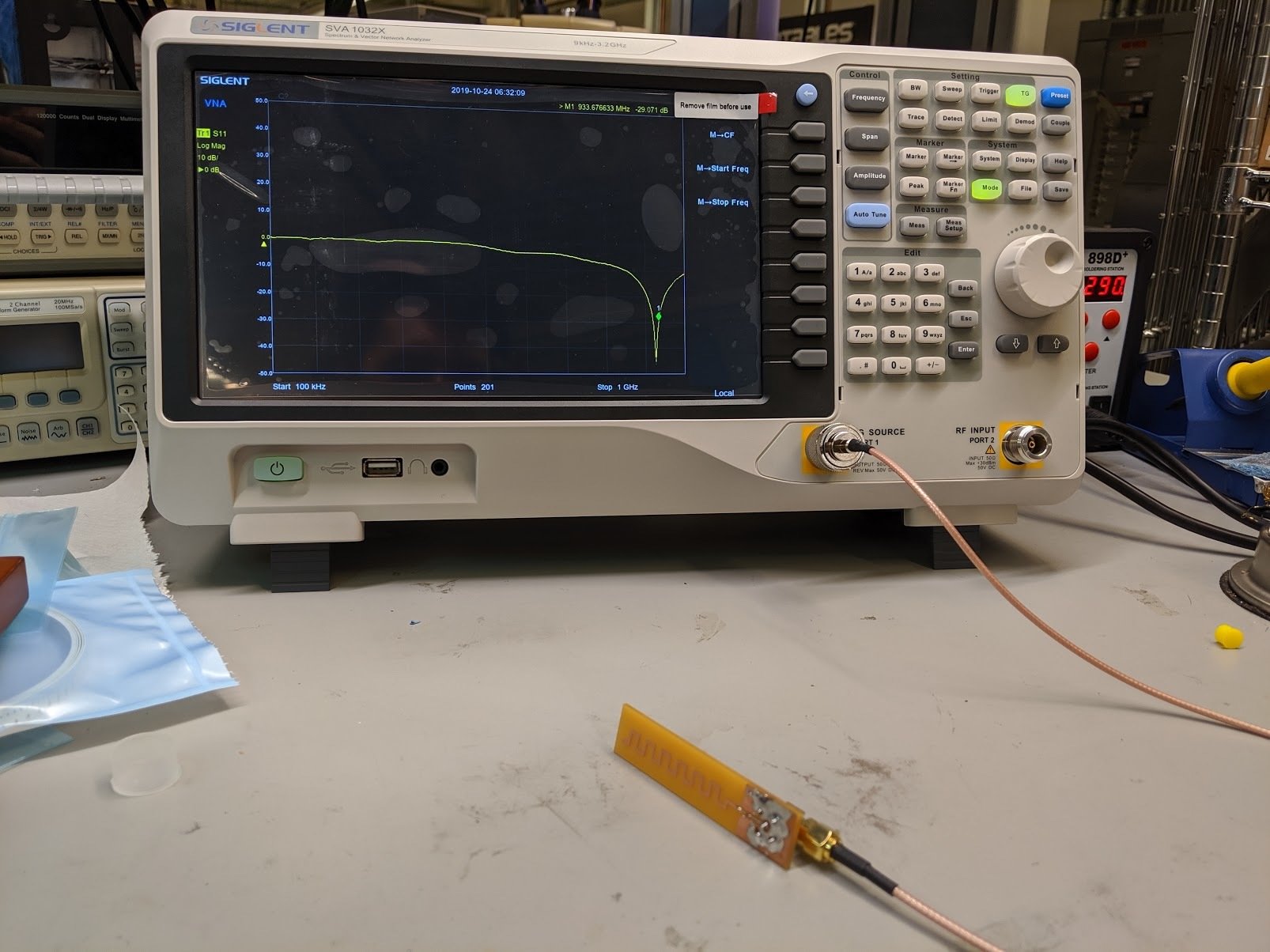
Testing with a VNA
Helped to get a feel for VNA Measurements
- Where was the resonant frequency and which frequencies will it transmit well? (SWR and Insertion Loss)
- How well matched was the antenna at my target frequency? (Smith Chart)
Getting a feel for good and bad antenna designs
- Good: Off the shelf antennas
- Bad: Just about anything I designed by myself
Understanding other constraints for VNAs
- Connectors
- Cables
- Calibration
What "DC" assumptions fall apart at higher frequencies?
-
A wire is just a wire
-
PCBs construction isn't as important as the components placed on that PCB
-
A capacitor is there for charge storage
-
Current can be isolated by ground cuts
-
Current follows the path of least resistance
"A wire is just a wire"
Actually every wire is an inductor


http://tiny.cc/Inductor_QR
What does this mean for our circuit?
Simple example:
Past 10 MHz, breadboard signal quality falls off

Image courtesy makerspaces.com
"PCBs construction isn't as important as the components placed on that PCB"

4 Layer Stackup
The PCB stackup impacts every piece of your signal pathways, including the impedance/inductance/capacitance of each stripline.
More complex PCB example:
In the GHz range, the small inductance of a PCB trace can have outsized effects on your signal

- Track width: 0.1 mm (3.94 mil)
- Track length: 50 mm (1.97 in)
- Height above GND: 0.2 mm (7.87 mil)
- Track inductance: 63.2 nH
- Impedance @ 2.4GHz: 953 ohm

http://tiny.cc/AAC_impedance
Ground plane should always be the layer below where your signal is running
Understanding your stackup is critical for treating your PCB as part of your circuit

https://tiny.cc/Stackup_JLC
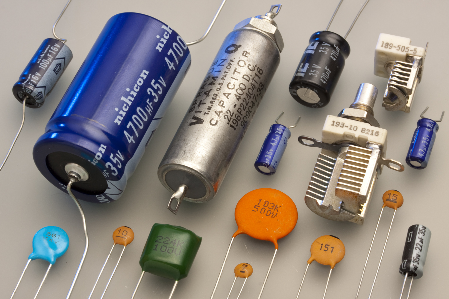
"A capacitor is there for charge storage"


Image courtesy of Wikipedia
Image courtesy of iFuture Technology
http://tiny.cc/KemetCapPDF
http://tiny.cc/KemetCapPDF
"Current can be isolated by ground cuts"
Noise reduction techniques in low level analog involves cutting the ground plane to stop noise from "leaking" over

https://www.analog.com/en/analog-dialogue/articles/staying-well-grounded.html
At low frequencies, the cutout means that the signals won't "get around" the cut, effectively shielding the isolated areas
High speed signals will treat this area as a capacitor and effectively "travel through" to the other side.
They often radiate energy while doing so. This is how we make PCB antennas (!)

"Current follows the path of least resistance"
The signal actually cares about the path of least impedance.
At DC, this is the path of least resistance.

http://tiny.cc/ECE_SE_highspeed
In higher speed signals, the impedance takes on more complex terms and the inductance starts to matter more.
The magnetic fields between two signals flowing in opposite directions cancel out

This means the inductance will be lowest directly below the signal path and the signal will preferentially flow black on the ground plane
http://tiny.cc/EIU_edu_wires
What about Bluetooth, Cellular, Wifi, LoRa, _______, etc, etc?
All of these communication methods are different versions of the same fundamentals
(and most are really brand names)
- Bluetooth - 2.4 GHz
- WiFi - 2.4 GHz and 5 GHz
-
LoRa, SigFox
- 433 MHz (Global)
- 915 MHz (US)
- 868 MHz (Europe)
-
GSM Cellular
- 900, 1800 MHz (Europe, Asia)
- 850, 1900 MHz (US)
-
3G, LTE, 5G
- Various frequencies (see: http://tiny.cc/cellular_freq)
Resources
Books
-
"A Practical Guide To RF And Mixed Signal Printed Circuit Board Layout" - Brendon Parise and Scott Nance[1]
- "RF Circuit Design" - Christopher Bowick [2]
- "Planar Microwave Engineering" - Thomas Lee [3]
[1]: https://amzn.to/2ZdnUzm
[2]: https://amzn.to/2HmQwey
[3]: https://amzn.to/2HnSWcY
YouTube
- W2AEW - https://www.youtube.com/user/w2aew
- The Signal Path - https://youtu.be/LN9PKKdFibo
Development kits/programs
- RTL-SDR + GNU Radio
- GSG HackRF
- ADI Pluto
Learning is critical to my job as a consultant
I want to learn things quickly so I can apply them for clients
I'd love to talk to people about:
-
RF testing
-
Connectivity options
-
Low cost microcontrollers
-
AWS IOT implementations
Thank you!
Twitter: @Chris_Gammell
E-mail: chris@analoglife.co
Many thanks to Jeff Keyzer (@mightyohm) and Derek Kozel (@derekkozel) for reviewing this presentation
Gaining RF Knowledge: An Analog Engineer Dives into RF Circuits
By Chris Gammell
Gaining RF Knowledge: An Analog Engineer Dives into RF Circuits
Hackaday Superconference 2019

