Electronics
Differential Amplifier

click here to move forward

This presentation will cover...


What is inside of an Op Amp?
(click me)
This is a long presentation...
Do some breaks between parts...

If you need an Op Amp brief review...
If you are familiar with Op Amps...

(click me)
(click me)
Before continuing...


Brief Op Amp Description...

It is a 5 terminal element.

Positive Input
Negative Input
Output
(Vcc or V+)
\( V_P \)
\(V_N\)
Positive Power Supply
Negative Power Supply
(Vee or V-)
Note: click on the arrows
The power supply can sometimes be excluded from the symbol...
Explicit Power Supply

Implicit Power Supply
(3 terminal element)
(5 terminal element)
Op Amps can be connected...
(click me)
(click me)


Open Loop
Op Amp behaves as a comparator...
(Circuit Link)
V_{out}=\left( V_P-V_N \right)\cdot A
Open Loop Gain (very high)
Output Saturates all the time either to Vcc or Vee
Note: click on the arrows
With Feedback
(click me)
(click me)
Positive Feedback...
(Circuit Link)

Behaves similar to the Op Amp in comparator but it introduces two points of comparison rather than one.
Negative Feedback...
Inverter
Goal: control the output gain and perform math operations.


Non-Inverter

Summing

Difference

Buffer
Part 1
(Building a Comparator)
Our First Goal...


Build a comparator...
...with BJTs
If you need a BJT configurations review...
(click me)
BJT Modes...
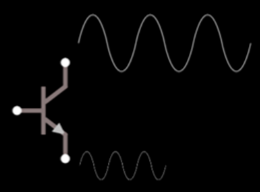
Amplifiers
Saturation or Cut Off
Active
(click me)
(click me)

(click me)
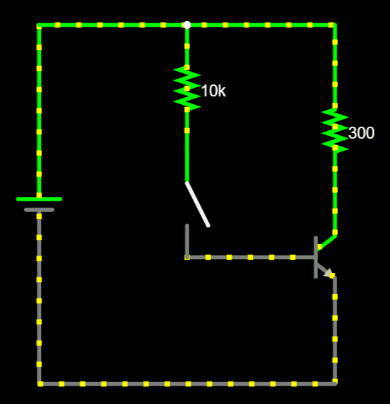
On/Off Configurations...
Note: click on each name to see a circuit example.
On/Off Configurations...
Note: click on each name to see a circuit example.
-
Digital Logic
-
H-Bridge
-
Oscillators
-
Switches
(Circuit Link)

(RTL NAND)
On/Off Configurations...
Note: click on each name to see a circuit example.
-
Digital Logic
-
H-Bridge
-
Oscillators
-
Switches
(Circuit Link)
(Colpitts)

On/Off Configurations...
Note: click on each name to see a circuit example.
-
Digital Logic
-
H-Bridge
-
Oscillators
-
Switches
(Under Development)
(Circuit Link)
On/Off Configurations...
Note: click on each name to see a circuit example.
-
Digital Logic
-
H-Bridge
-
Oscillators
-
Switches
(Circuit Link)
Common Configurations...


b
c
e
Individual transistor
Multistage Configurations...
Note: click on each name to see a circuit example.
Two or more transistors
Multistage Configurations...
-
Darlington
-
Differential
-
Push-Pull
-
Current Mirror
(Circuit Link)


Note: click on each name to see a circuit example.
Two or more transistors
Multistage Configurations...
-
Darlington
-
Differential
-
Push-Pull
-
Current Mirror
Note: click on each name to see a circuit example.
Two or more transistors


(Circuit Link)
Multistage Configurations...
-
Darlington
-
Differential
-
Push-Pull
-
Current Mirror
Note: click on each name to see a circuit example.
Two or more transistors
(Circuit Link)


Multistage Configurations...
-
Darlington
-
Differential
-
Push-Pull
-
Current Mirror
Note: click on each name to see a circuit example.
Two or more transistors
(Circuit Link)


From the Comparator Equation...
We want to perform a subtraction and amplify that result.
V_{out}= \color{lime} \left( V_P-V_N \right) \color{cyan} \cdot A
Open Loop Gain (very high)
Let's start by using a single transistor first (common configuration)
(click me)
From the 3 Common Configurations...
CE and CB are suitable for amplification...
(click me)
(click me)
(click me)
CE Simulation

Signal in
Signal out

(Circuit Link)

\color{red} V_{out}
\color{lime} V_{in}

\color{red} V_{out} = \color{lime} - V_{in}
Improved Version with Amplification
CB Simulation
Signal out
Signal in

\color{red} V_{out}
\color{lime} V_{in}
\color{red} V_{out} = \color{lime} V_{in}
(Circuit Link)
CC Simulation
Signal out
Signal in


(Circuit Link)
The Comparator
Has 2 inputs and 1 output...
But CE and CB have only 1 input and 1 output...
Signal out
Signal in
Signal in
Signal out
\color{red} V_{out}
\color{lime} V_{p}
\color{lime} V_{n}
The Comparator
What if we combine CE with CB...
Signal out
Signal in
Signal in
Signal out
\color{red} V_{out} = \color{lime} - V_{in}
\color{red} V_{out} = \color{lime} V_{in}
\color{red} V_{out}
\color{lime} V_{p}
\color{lime} V_{n}

(click me)
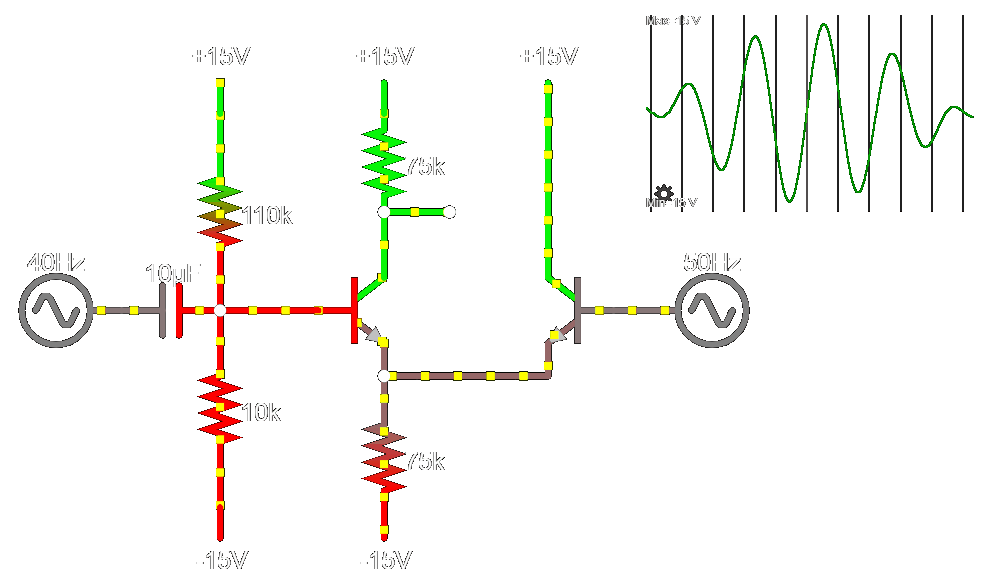
Signal is on the Current too...
Notice on how the \(V_{BE}\) of the transistor performs the subtraction between the inputs...
\color{lime} V_{p}
\color{lime} V_{n}
V_{BE} = V_B - V_E = V_n - V_p
I_{B} = I_s \cdot e^{\frac{V_{BE}}{V_T}}
And that \(V_{BE}\) is reflected on the transistor current...
I_{C} = \beta \cdot I_{B}
Let's Simulate...

\color{lime} V_{p}
\color{lime} V_{n}
\color{red} V_{out}

(click me)
Expected Result
(click me)
Saturating: Bias Issue
(Circuit Link)
(More detailed explanation here)
Expected Result

V_{out} = sin(2\pi 50t) - sin(2\pi 40t)
More Detail...

(Circuit Link)
Good signal at \(V_{BE}\)
V_{out} = V_{CC} - I_C \cdot R
Signal too close to \(V_{CC}\)
Output Saturated
Iteration 1...
\color{lime} V_{p}
\color{lime} V_{n}
\color{red} V_{out}
(Circuit Link)

(click me)
DC Coupling issue
Bias circuit added
Iteration 2...
\color{lime} V_{p}
\color{lime} V_{n}
\color{red} V_{out}
(Circuit Link)
AC Coupled

Impedance issue
(click me)
Iteration 3...
\color{lime} V_{p}
\color{lime} V_{n}
\color{red} V_{out}

Fix Impedance
Iteration 3...
\color{lime} V_{p}
\color{lime} V_{n}
\color{red} V_{out}
Impedance Fixed
(Circuit Link)
(click me)
Bias issue again
Iteration 3...
\color{lime} V_{p}
\color{lime} V_{n}
\color{red} V_{out}
Bias fixed
(Circuit Link)

(click me)
Interesting Fact...
Interesting Fact...
\color{lime} V_{p}
\color{lime} V_{n}
\color{red} V_{out}
(Circuit Link)

If we instead DC couple the now symmetric inputs the biasing becomes unnecessary...

Iteration 4...
\color{lime} V_{p}
\color{lime} V_{n}
\color{red} V_{out}
Good enough
DC Coupled
(Circuit Link)
Expected Result
Bias Resistors Removed
Differential Amplifier (Single End)
\color{lime} V_{p}
\color{lime} V_{n}
\color{red} V_{out} \color{white} = \color{lime} V_n - V_p
(Circuit Link)
Test with Different Inputs...
\color{lime} V_{p} = sin(2\pi 40t) + sin(2\pi 200t)
\color{lime} V_{n} = sin(2\pi 40t)
\color{red} V_{out} = -sin(2\pi 200t)
(Circuit Link)
V_{out} = V_n - V_p

Long-Tailed Pair
\color{lime} V_{p}
\color{lime} V_{n}
(Circuit Link)
\color{red} V_{out1} \color{white} = \color{lime} V_n - V_p
\color{red} V_{out2} \color{white} = \color{lime} V_p - V_n
(Two Outputs)

Part 2
(Building Op Amp Stages)
Do a break if needed...
Steps...
1. Improve the Single End Configuration
2. Build the First Stage
3. Build the Second Stage
4. Build the Third Stage
5. Some Adjustments
Challenges
Resistors Noise
Load Impedance
(click me)
(click me)

Resistors Noise
Can we minimize the resistors noise?
(click me)
Resistors Noise
Johnson-Nyquist noise or thermal noise, is the electronic noise generated by the thermal agitation of the charge carriers inside an electrical conductor at equilibrium.

Thermal noise is present in all electrical circuits.


(click me)
Resistors Noise Model
We can include a model of the Johnson-Nyquist noise into any circuit simulation...


Electronics_Differential_Amplifier
By Goncalo Martins
Electronics_Differential_Amplifier
Differential Amplifier Explanation


