What is RGMII?
Chen Zhang, Wenhou Sun, Xingyu Xie
MII(Medium-independent Interface)
Connects different types of PHYs to MACs.
Standardized by IEEE 802.3u.
GMII(Gigabit MII)
Speeds up to 1000Mbit/s, clocked at 125MHZ.
Standardized by IEEE 802.3-2000
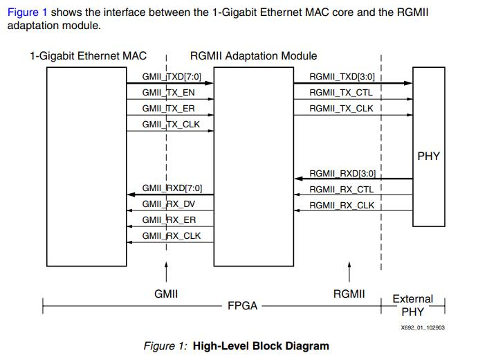
RGMII(Reduced GMII)
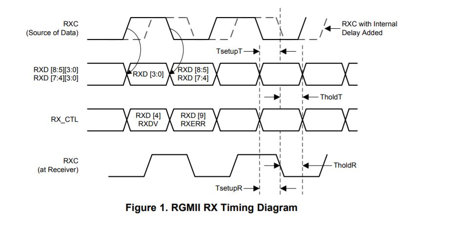
Use half the number of data pins as used in the GMII.
This reduction is achieved by clocking data on both the rising and falling edges of the clock in 1000Mbit/s operation, and by eliminating non-essential signals.
Signals of RGMII
| Signal name | Description | Direction |
|---|---|---|
| TXC | Clock signal | MAC to PHY |
| TXD[3..0] | Data to be transmitted | MAC to PHY |
| TX_CTL | Multiplexing of transmitter enable and transmitter error | MAC to PHY |
| RXC | Received clock signal (recovered from incoming received data) | PHY to MAC |
| RXD[3..0] | Received data | PHY to MAC |
| RX_CTL |
Multiplexing of data received is valid and receiver error | PHY to MAC |
| MDC | Management interface clock | MAC to PHY |
| MDIO | Management interface I/O | Bidirectional |
Thanks!
MMI
By Xingyu Xie
MMI
A presentationi to introduce MMI


